

212
T. T.-H. Kim
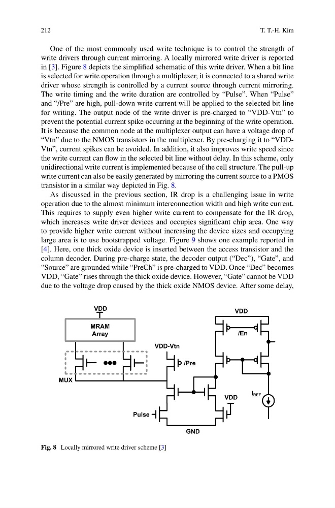
One of the most commonly used write technique is to control the strength of
write drivers through current mirroring. A locally mirrored write driver is reported
in [3]. Figure 8 depicts the simplified schematic of this write driver. When a bit line
is selected for write operation through a multiplexer, it is connected to a shared write
driver whose strength is controlled by a current source through current mirroring.
The write timing and the write duration are controlled by “Pulse”. When “Pulse”
and “/Pre” are high, pull-down write current will be applied to the selected bit line
for writing. The output node of the write driver is pre-charged to “VDD-Vtn” to
prevent the potential current spike occurring at the beginning of the write operation.
It is because the common node at the multiplexer output can have a voltage drop of
“Vtn” due to the NMOS transistors in the multiplexer. By pre-charging it to “VDDVtn”, current spikes can be avoided. In addition, it also improves write speed since
the write current can flow in the selected bit line without delay. In this scheme, only
unidirectional write current is implemented because of the cell structure. The pull-up
write current can also be easily generated by mirroring the current source to a PMOS
transistor in a similar way depicted in Fig. 8.
As discussed in the previous section, IR drop is a challenging issue in write
operation due to the almost minimum interconnection width and high write current.
This requires to supply even higher write current to compensate for the IR drop,
which increases write driver devices and occupies significant chip area. One way
to provide higher write current without increasing the device sizes and occupying
large area is to use bootstrapped voltage. Figure 9 shows one example reported in
[4]. Here, one thick oxide device is inserted between the access transistor and the
column decoder. During pre-charge state, the decoder output (“Dec”), “Gate”, and
“Source” are grounded while “PreCh” is pre-charged to VDD. Once “Dec” becomes
VDD, “Gate” rises through the thick oxide device. However, “Gate” cannot be VDD
due to the voltage drop caused by the thick oxide NMOS device. After some delay,
MRAM
Array
VDD
VDD
VDD
I REF
VDD-Vtn
/Pre
/En
Pulse
MUX
GND
Fig. 8 Locally mirrored write driver scheme [3]
T. T.-H. Kim
One of the most commonly used write technique is to control the strength of
write drivers through current mirroring. A locally mirrored write driver is reported
in [3]. Figure 8 depicts the simplified schematic of this write driver. When a bit line
is selected for write operation through a multiplexer, it is connected to a shared write
driver whose strength is controlled by a current source through current mirroring.
The write timing and the write duration are controlled by “Pulse”. When “Pulse”
and “/Pre” are high, pull-down write current will be applied to the selected bit line
for writing. The output node of the write driver is pre-charged to “VDD-Vtn” to
prevent the potential current spike occurring at the beginning of the write operation.
It is because the common node at the multiplexer output can have a voltage drop of
“Vtn” due to the NMOS transistors in the multiplexer. By pre-charging it to “VDDVtn”, current spikes can be avoided. In addition, it also improves write speed since
the write current can flow in the selected bit line without delay. In this scheme, only
unidirectional write current is implemented because of the cell structure. The pull-up
write current can also be easily generated by mirroring the current source to a PMOS
transistor in a similar way depicted in Fig. 8.
As discussed in the previous section, IR drop is a challenging issue in write
operation due to the almost minimum interconnection width and high write current.
This requires to supply even higher write current to compensate for the IR drop,
which increases write driver devices and occupies significant chip area. One way
to provide higher write current without increasing the device sizes and occupying
large area is to use bootstrapped voltage. Figure 9 shows one example reported in
[4]. Here, one thick oxide device is inserted between the access transistor and the
column decoder. During pre-charge state, the decoder output (“Dec”), “Gate”, and
“Source” are grounded while “PreCh” is pre-charged to VDD. Once “Dec” becomes
VDD, “Gate” rises through the thick oxide device. However, “Gate” cannot be VDD
due to the voltage drop caused by the thick oxide NMOS device. After some delay,
MRAM
Array
VDD
VDD
VDD
I REF
VDD-Vtn
/Pre
/En
Pulse
MUX
GND
Fig. 8 Locally mirrored write driver scheme [3]