

Circuit Design for Non-volatile Magnetic Memory
211
in the crossbar array architecture where multiple cells undergo certain bias voltage.
The bias voltage is maintained below the threshold level so that no disturbance
on the cell resistance occurs. However, the long term reliability of those magnetic
memory cells need to be further investigated. Finally, sneak current is inevitable in
the available magnetic memory array architectures. It affects, write current, IR drop,
MTJ reliability, and overall power consumption. Two popular bias schemes are based
upon the trade-off in the MTJ reliability and the power consumption.
5 Write Techniques for Magnetic Memory
Magnetic memory has been considered as a promising candidate for replacing
SRAMs and DRAMs. However, one of the most critical issues is the large write
current. In addition, variations in the characteristics of fabricated MTJ devices
increase the write current even more to provide enough margins for write operation. It is important to control write current carefully for successful write operation
without significant disturbance and power consumption. While simply increasing
the size of the selection transistor is the easiest method for reducing write failures,
it limits the scalability of the memory. In addition, the write pulse width also needs
to be carefully selected to reduce power consumption without dramatic increase in
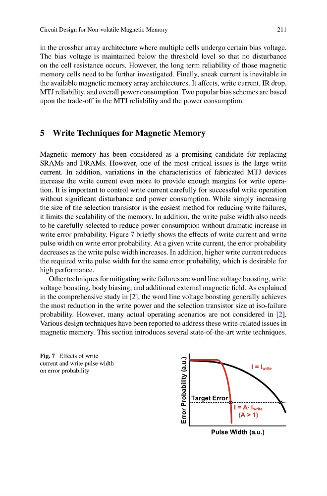
write error probability. Figure 7 briefly shows the effects of write current and write
pulse width on write error probability. At a given write current, the error probability
decreases as the write pulse width increases. In addition, higher write current reduces
the required write pulse width for the same error probability, which is desirable for
high performance.
Other techniques for mitigating write failures are word line voltage boosting, write
voltage boosting, body biasing, and additional external magnetic field. As explained
in the comprehensive study in [2], the word line voltage boosting generally achieves
the most reduction in the write power and the selection transistor size at iso-failure
probability. However, many actual operating scenarios are not considered in [2].
Various design techniques have been reported to address these write-related issues in
magnetic memory. This section introduces several state-of-the-art write techniques.
Fig. 7 Effects of write
current and write pulse width
on error probability
Pulse Width (a.u.)
Error Probability (a.u.)
I = A· I write
(A > 1)
I = I write
Target Error
211
in the crossbar array architecture where multiple cells undergo certain bias voltage.
The bias voltage is maintained below the threshold level so that no disturbance
on the cell resistance occurs. However, the long term reliability of those magnetic
memory cells need to be further investigated. Finally, sneak current is inevitable in
the available magnetic memory array architectures. It affects, write current, IR drop,
MTJ reliability, and overall power consumption. Two popular bias schemes are based
upon the trade-off in the MTJ reliability and the power consumption.
5 Write Techniques for Magnetic Memory
Magnetic memory has been considered as a promising candidate for replacing
SRAMs and DRAMs. However, one of the most critical issues is the large write
current. In addition, variations in the characteristics of fabricated MTJ devices
increase the write current even more to provide enough margins for write operation. It is important to control write current carefully for successful write operation
without significant disturbance and power consumption. While simply increasing
the size of the selection transistor is the easiest method for reducing write failures,
it limits the scalability of the memory. In addition, the write pulse width also needs
to be carefully selected to reduce power consumption without dramatic increase in
write error probability. Figure 7 briefly shows the effects of write current and write
pulse width on write error probability. At a given write current, the error probability
decreases as the write pulse width increases. In addition, higher write current reduces
the required write pulse width for the same error probability, which is desirable for
high performance.
Other techniques for mitigating write failures are word line voltage boosting, write
voltage boosting, body biasing, and additional external magnetic field. As explained
in the comprehensive study in [2], the word line voltage boosting generally achieves
the most reduction in the write power and the selection transistor size at iso-failure
probability. However, many actual operating scenarios are not considered in [2].
Various design techniques have been reported to address these write-related issues in
magnetic memory. This section introduces several state-of-the-art write techniques.
Fig. 7 Effects of write
current and write pulse width
on error probability
Pulse Width (a.u.)
Error Probability (a.u.)
I = A· I write
(A > 1)
I = I write
Target Error