

210
T. T.-H. Kim
the cells in the unselected columns and the unselected rows see the voltage difference
of 1/3V W . Therefore, it can be expected that the magnetic memory cells will have
less disturbance in their resistance. However, all the cells except the selected cell
see 1/3V W , generating more sneak current. Overall, this scheme is preferred when
device reliability is a more serious concern than power consumption.
4 Design Challenges of Magnetic Memory
This section briefly summarizes general design challenges in magnetic memory. The
issues include low TMR ratios, small sensing margins, large write current, IR drop in
the interconnection, MTJ reliability, sneak current, etc. Many of the above issues are
not independent but interrelated. One of the most critical issue in designing magnetic
memory is the low TMR ratio. This is a similar to the on-current to off-current ratio
of a transistor, conceptually. In general, the TMR ratio is <200% even though higher
TMR ratios have been achieved in some recent research works. Other emerging
memory devices such as PCRAM and RRAM usually show much higher on-to-off
resistance ratios, which provides relatively large sensing margins. The low TMR
ratio imposes more challenges in sensing circuit design. Write current is another
significant issue that needs to be addressed in the magnetic memory design. As
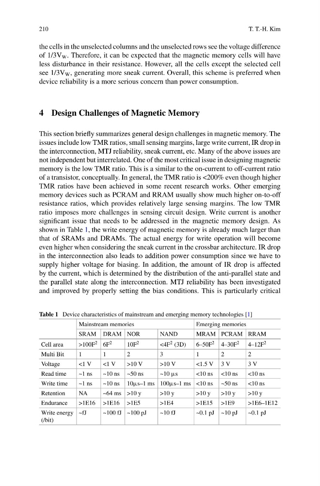
shown in Table 1, the write energy of magnetic memory is already much larger than
that of SRAMs and DRAMs. The actual energy for write operation will become
even higher when considering the sneak current in the crossbar architecture. IR drop
in the interconnection also leads to addition power consumption since we have to
supply higher voltage for biasing. In addition, the amount of IR drop is affected
by the current, which is determined by the distribution of the anti-parallel state and
the parallel state along the interconnection. MTJ reliability has been investigated
and improved by properly setting the bias conditions. This is particularly critical
Table 1 Device characteristics of mainstream and emerging memory technologies [1]
Mainstream memories
Emerging memories
SRAM DRAM NOR
NAND
MRAM PCRAM RRAM
Cell area
>100F 2 6F 2
10F 2
<4F 2 (3D)
6–50F 2 4–30F 2 4–12F 2
Multi Bit
1
1
2
3
1
2
2
Voltage
<1 V
<1 V
>10 V
>10 V
<1.5 V 3 V
3 V
Read time
~1 ns
~10 ns ~50 ns
~10 µs
<10 ns <10 ns
<10 ns
Write time
~1 ns
~10 ns 10µs–1 ms 100µs–1 ms <10 ns ~50 ns
<10 ns
Retention
NA
~64 ms >10 y
>10 y
>10 y
>10 y
>10 y
Endurance
>1E16 >1E16 >1E5
>1E4
>1E15 >1E9
>1E6–1E12
Write energy
(/bit)
~fJ
~100 fJ ~100 pJ
~10 fJ
~0.1 pJ ~10 pJ
~0.1 pJ
T. T.-H. Kim
the cells in the unselected columns and the unselected rows see the voltage difference
of 1/3V W . Therefore, it can be expected that the magnetic memory cells will have
less disturbance in their resistance. However, all the cells except the selected cell
see 1/3V W , generating more sneak current. Overall, this scheme is preferred when
device reliability is a more serious concern than power consumption.
4 Design Challenges of Magnetic Memory
This section briefly summarizes general design challenges in magnetic memory. The
issues include low TMR ratios, small sensing margins, large write current, IR drop in
the interconnection, MTJ reliability, sneak current, etc. Many of the above issues are
not independent but interrelated. One of the most critical issue in designing magnetic
memory is the low TMR ratio. This is a similar to the on-current to off-current ratio
of a transistor, conceptually. In general, the TMR ratio is <200% even though higher
TMR ratios have been achieved in some recent research works. Other emerging
memory devices such as PCRAM and RRAM usually show much higher on-to-off
resistance ratios, which provides relatively large sensing margins. The low TMR
ratio imposes more challenges in sensing circuit design. Write current is another
significant issue that needs to be addressed in the magnetic memory design. As
shown in Table 1, the write energy of magnetic memory is already much larger than
that of SRAMs and DRAMs. The actual energy for write operation will become
even higher when considering the sneak current in the crossbar architecture. IR drop
in the interconnection also leads to addition power consumption since we have to
supply higher voltage for biasing. In addition, the amount of IR drop is affected
by the current, which is determined by the distribution of the anti-parallel state and
the parallel state along the interconnection. MTJ reliability has been investigated
and improved by properly setting the bias conditions. This is particularly critical
Table 1 Device characteristics of mainstream and emerging memory technologies [1]
Mainstream memories
Emerging memories
SRAM DRAM NOR
NAND
MRAM PCRAM RRAM
Cell area
>100F 2 6F 2
10F 2
<4F 2 (3D)
6–50F 2 4–30F 2 4–12F 2
Multi Bit
1
1
2
3
1
2
2
Voltage
<1 V
<1 V
>10 V
>10 V
<1.5 V 3 V
3 V
Read time
~1 ns
~10 ns ~50 ns
~10 µs
<10 ns <10 ns
<10 ns
Write time
~1 ns
~10 ns 10µs–1 ms 100µs–1 ms <10 ns ~50 ns
<10 ns
Retention
NA
~64 ms >10 y
>10 y
>10 y
>10 y
>10 y
Endurance
>1E16 >1E16 >1E5
>1E4
>1E15 >1E9
>1E6–1E12
Write energy
(/bit)
~fJ
~100 fJ ~100 pJ
~10 fJ
~0.1 pJ ~10 pJ
~0.1 pJ