

Circuit Design for Non-volatile Magnetic Memory
209
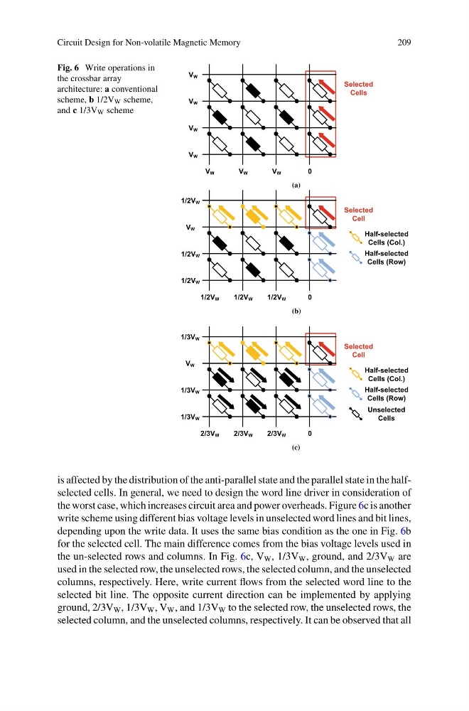
Fig. 6 Write operations in
the crossbar array
architecture: a conventional
scheme, b 1/2V W scheme,
and c 1/3V W scheme
VW
VW
VW
VW
VW
VW
VW
0
Selected
Cells
(a)
1/2VW
VW
1/2VW
1/2VW
1/2VW
1/2VW
1/2VW
0
Selected
Cell
Half-selected
Cells (Col.)
Half-selected
Cells (Row)
(b)
1/3VW
VW
1/3VW
1/3VW
2/3VW
2/3VW
2/3VW
0
Selected
Cell
Half-selected
Cells (Col.)
Half-selected
Cells (Row)
Unselected
Cells
(c)
is affected by the distribution of the anti-parallel state and the parallel state in the halfselected cells. In general, we need to design the word line driver in consideration of
the worst case, which increases circuit area and power overheads. Figure 6c is another
write scheme using different bias voltage levels in unselected word lines and bit lines,
depending upon the write data. It uses the same bias condition as the one in Fig. 6b
for the selected cell. The main difference comes from the bias voltage levels used in
the un-selected rows and columns. In Fig. 6c, V W , 1/3V W , ground, and 2/3V W are
used in the selected row, the unselected rows, the selected column, and the unselected
columns, respectively. Here, write current flows from the selected word line to the
selected bit line. The opposite current direction can be implemented by applying
ground, 2/3V W , 1/3V W , V W , and 1/3V W to the selected row, the unselected rows, the
selected column, and the unselected columns, respectively. It can be observed that all
209
Fig. 6 Write operations in
the crossbar array
architecture: a conventional
scheme, b 1/2V W scheme,
and c 1/3V W scheme
VW
VW
VW
VW
VW
VW
VW
0
Selected
Cells
(a)
1/2VW
VW
1/2VW
1/2VW
1/2VW
1/2VW
1/2VW
0
Selected
Cell
Half-selected
Cells (Col.)
Half-selected
Cells (Row)
(b)
1/3VW
VW
1/3VW
1/3VW
2/3VW
2/3VW
2/3VW
0
Selected
Cell
Half-selected
Cells (Col.)
Half-selected
Cells (Row)
Unselected
Cells
(c)
is affected by the distribution of the anti-parallel state and the parallel state in the halfselected cells. In general, we need to design the word line driver in consideration of
the worst case, which increases circuit area and power overheads. Figure 6c is another
write scheme using different bias voltage levels in unselected word lines and bit lines,
depending upon the write data. It uses the same bias condition as the one in Fig. 6b
for the selected cell. The main difference comes from the bias voltage levels used in
the un-selected rows and columns. In Fig. 6c, V W , 1/3V W , ground, and 2/3V W are
used in the selected row, the unselected rows, the selected column, and the unselected
columns, respectively. Here, write current flows from the selected word line to the
selected bit line. The opposite current direction can be implemented by applying
ground, 2/3V W , 1/3V W , V W , and 1/3V W to the selected row, the unselected rows, the
selected column, and the unselected columns, respectively. It can be observed that all