

208
T. T.-H. Kim
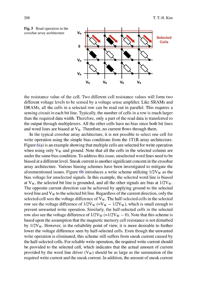
Fig. 5 Read operation in the
crossbar array architecture
V R
0
V R
V R
V R
V R
V R
V R
Selected
Cells
the resistance value of the cell. Two different cell resistance values will form two
different voltage levels to be sensed by a voltage sense amplifier. Like SRAMs and
DRAMs, all the cells in a selected row can be read out in parallel. This requires a
sensing circuit in each bit line. Typically, the number of cells in a row is much larger
than the required data width. Therefore, only a part of the read data is transferred to
the output through multiplexers. All the other cells have no bias since both bit lines
and word lines are biased at V R . Therefore, no current flows through them.
In the typical crossbar array architecture, it is not possible to select one cell for
write operation using the simple bias conditions from the 1T1R array architecture.
Figure 6(a) is an example showing that multiple cells are selected for write operation
when using only V W and ground. Note that all the cells in the selected column are
under the same bias condition. To address this issue, unselected word lines need to be
biased at a different level. Sneak current is another significant concern in the crossbar
array architecture. Various biasing schemes have been investigated to mitigate the
aforementioned issues. Figure 6b introduces a write scheme utilizing 1/2V W as the
bias voltage for unselected signals. In this example, the selected word line is biased
at V W , the selected bit line is grounded, and all the other signals are bias at 1/2V W .
The opposite current direction can be achieved by applying ground to the selected
word line and V W to the selected bit line. Regardless of the current direction, only the
selected cell sees the voltage difference of V W . The half-selected cells in the selected
row see the voltage difference of 1/2V W (=V W − 1/2V W ), which is small enough to
prevent unwanted write operation. Similarly, the half-selected cells in the selected
row also see the voltage difference of 1/2V W (=1/2V W − 0). Note that this scheme is
based upon the assumption that the magnetic memory cell resistance is not disturbed
by 1/2V W . However, in the reliability point of view, it is more desirable to further
lower the voltage difference seen by half-selected cells. Even though the unwanted
write operation is eliminated, this scheme still suffers from sneak current caused by
the half-selected cells. For reliable write operation, the required write current should
be provided to the selected cell, which indicates that the actual amount of current
provided by the word line driver (V W ) should be as large as the summation of the
required write current and the sneak current. In addition, the amount of sneak current
T. T.-H. Kim
Fig. 5 Read operation in the
crossbar array architecture
V R
0
V R
V R
V R
V R
V R
V R
Selected
Cells
the resistance value of the cell. Two different cell resistance values will form two
different voltage levels to be sensed by a voltage sense amplifier. Like SRAMs and
DRAMs, all the cells in a selected row can be read out in parallel. This requires a
sensing circuit in each bit line. Typically, the number of cells in a row is much larger
than the required data width. Therefore, only a part of the read data is transferred to
the output through multiplexers. All the other cells have no bias since both bit lines
and word lines are biased at V R . Therefore, no current flows through them.
In the typical crossbar array architecture, it is not possible to select one cell for
write operation using the simple bias conditions from the 1T1R array architecture.
Figure 6(a) is an example showing that multiple cells are selected for write operation
when using only V W and ground. Note that all the cells in the selected column are
under the same bias condition. To address this issue, unselected word lines need to be
biased at a different level. Sneak current is another significant concern in the crossbar
array architecture. Various biasing schemes have been investigated to mitigate the
aforementioned issues. Figure 6b introduces a write scheme utilizing 1/2V W as the
bias voltage for unselected signals. In this example, the selected word line is biased
at V W , the selected bit line is grounded, and all the other signals are bias at 1/2V W .
The opposite current direction can be achieved by applying ground to the selected
word line and V W to the selected bit line. Regardless of the current direction, only the
selected cell sees the voltage difference of V W . The half-selected cells in the selected
row see the voltage difference of 1/2V W (=V W − 1/2V W ), which is small enough to
prevent unwanted write operation. Similarly, the half-selected cells in the selected
row also see the voltage difference of 1/2V W (=1/2V W − 0). Note that this scheme is
based upon the assumption that the magnetic memory cell resistance is not disturbed
by 1/2V W . However, in the reliability point of view, it is more desirable to further
lower the voltage difference seen by half-selected cells. Even though the unwanted
write operation is eliminated, this scheme still suffers from sneak current caused by
the half-selected cells. For reliable write operation, the required write current should
be provided to the selected cell, which indicates that the actual amount of current
provided by the word line driver (V W ) should be as large as the summation of the
required write current and the sneak current. In addition, the amount of sneak current