

Circuit Design for Non-volatile Magnetic Memory
207
size (12 F
2 ) for the 1T1R array architecture is larger than the DRAM cell size (6
F
2 ) due to two significant requirements. First, the 1T1R array architecture has two
vertical lines (SLi and BLi) while the DRAM architecture has only one vertical line.
In addition, the amount of required write current also limits the cell size minimization. In general, the amount of write current generated by a minimum size selection transistor is not large enough for reliable write operation (SET and RESET).
Therefore, the transistor size should be increased, which also increase the magnetic
memory cell size, accordingly. To tackle this issue, the crossbar array architecture
has been introduced where no selection transistor is used as depicted in Fig. 3. In this
architecture, word lines (WL i ) and bit lines (BL i ) are connected perpendicularly and
magnetic memory cells are inserted between the word lines and the bit lines. The
crossbar array architecture has been reported to have the cell area of 4 F
2 because of
removing the selection transistor. Thus, the density of the magnetic memory in the
crossbar array architecture is higher than that of the magnetic memory in the 1T1R
array architecture and that of DRAMs. When compared to the 1T1R array architecture, the crossbar array architecture has no source lines. This prevents a selected
magnetic memory cell from being isolated from other unselected cells. To address
this issue, the crossbar array architecture typically employs magnetic memory cells
consisting of one selector and one MTJ (1S1R).
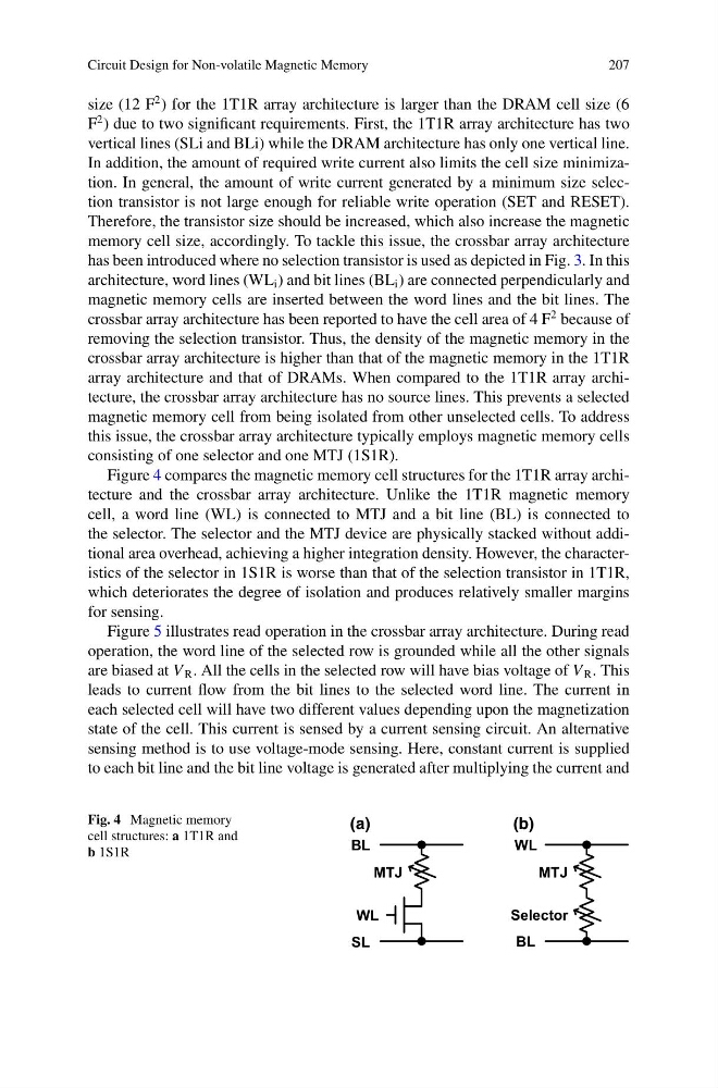
Figure 4 compares the magnetic memory cell structures for the 1T1R array architecture and the crossbar array architecture. Unlike the 1T1R magnetic memory
cell, a word line (WL) is connected to MTJ and a bit line (BL) is connected to
the selector. The selector and the MTJ device are physically stacked without additional area overhead, achieving a higher integration density. However, the characteristics of the selector in 1S1R is worse than that of the selection transistor in 1T1R,
which deteriorates the degree of isolation and produces relatively smaller margins
for sensing.
Figure 5 illustrates read operation in the crossbar array architecture. During read
operation, the word line of the selected row is grounded while all the other signals
are biased at V R . All the cells in the selected row will have bias voltage of V R . This
leads to current flow from the bit lines to the selected word line. The current in
each selected cell will have two different values depending upon the magnetization
state of the cell. This current is sensed by a current sensing circuit. An alternative
sensing method is to use voltage-mode sensing. Here, constant current is supplied
to each bit line and the bit line voltage is generated after multiplying the current and
Fig. 4 Magnetic memory
cell structures: a 1T1R and
b 1S1R
BL
(a)
(b)
SL
WL
MTJ
MTJ
Selector
WL
BL
207
size (12 F
2 ) for the 1T1R array architecture is larger than the DRAM cell size (6
F
2 ) due to two significant requirements. First, the 1T1R array architecture has two
vertical lines (SLi and BLi) while the DRAM architecture has only one vertical line.
In addition, the amount of required write current also limits the cell size minimization. In general, the amount of write current generated by a minimum size selection transistor is not large enough for reliable write operation (SET and RESET).
Therefore, the transistor size should be increased, which also increase the magnetic
memory cell size, accordingly. To tackle this issue, the crossbar array architecture
has been introduced where no selection transistor is used as depicted in Fig. 3. In this
architecture, word lines (WL i ) and bit lines (BL i ) are connected perpendicularly and
magnetic memory cells are inserted between the word lines and the bit lines. The
crossbar array architecture has been reported to have the cell area of 4 F
2 because of
removing the selection transistor. Thus, the density of the magnetic memory in the
crossbar array architecture is higher than that of the magnetic memory in the 1T1R
array architecture and that of DRAMs. When compared to the 1T1R array architecture, the crossbar array architecture has no source lines. This prevents a selected
magnetic memory cell from being isolated from other unselected cells. To address
this issue, the crossbar array architecture typically employs magnetic memory cells
consisting of one selector and one MTJ (1S1R).
Figure 4 compares the magnetic memory cell structures for the 1T1R array architecture and the crossbar array architecture. Unlike the 1T1R magnetic memory
cell, a word line (WL) is connected to MTJ and a bit line (BL) is connected to
the selector. The selector and the MTJ device are physically stacked without additional area overhead, achieving a higher integration density. However, the characteristics of the selector in 1S1R is worse than that of the selection transistor in 1T1R,
which deteriorates the degree of isolation and produces relatively smaller margins
for sensing.
Figure 5 illustrates read operation in the crossbar array architecture. During read
operation, the word line of the selected row is grounded while all the other signals
are biased at V R . All the cells in the selected row will have bias voltage of V R . This
leads to current flow from the bit lines to the selected word line. The current in
each selected cell will have two different values depending upon the magnetization
state of the cell. This current is sensed by a current sensing circuit. An alternative
sensing method is to use voltage-mode sensing. Here, constant current is supplied
to each bit line and the bit line voltage is generated after multiplying the current and
Fig. 4 Magnetic memory
cell structures: a 1T1R and
b 1S1R
BL
(a)
(b)
SL
WL
MTJ
MTJ
Selector
WL
BL