

206
T. T.-H. Kim
WLi
WL i+1
WLi+2
WLi+3
BLi
BLi+1
BLi+2
BLi+3
: '1' (Anti-parallel)
: '0' (Parallel)
States of MRAM Cell
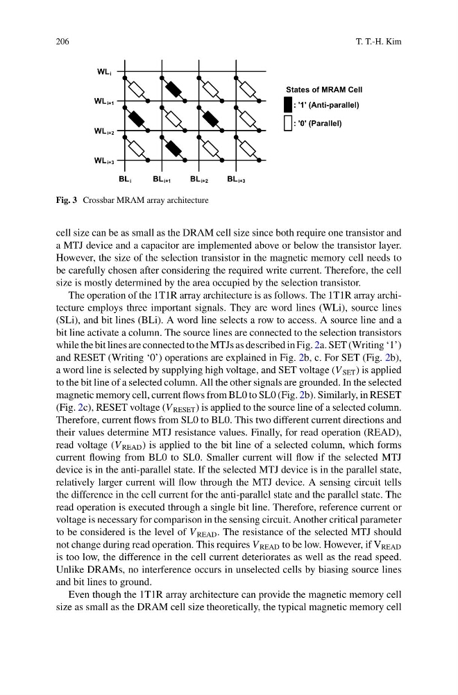
Fig. 3 Crossbar MRAM array architecture
cell size can be as small as the DRAM cell size since both require one transistor and
a MTJ device and a capacitor are implemented above or below the transistor layer.
However, the size of the selection transistor in the magnetic memory cell needs to
be carefully chosen after considering the required write current. Therefore, the cell
size is mostly determined by the area occupied by the selection transistor.
The operation of the 1T1R array architecture is as follows. The 1T1R array architecture employs three important signals. They are word lines (WLi), source lines
(SLi), and bit lines (BLi). A word line selects a row to access. A source line and a
bit line activate a column. The source lines are connected to the selection transistors
while the bit lines are connected to the MTJs as described in Fig. 2a. SET (Writing ‘1’)
and RESET (Writing ‘0’) operations are explained in Fig. 2b, c. For SET (Fig. 2b),
a word line is selected by supplying high voltage, and SET voltage (V SET ) is applied
to the bit line of a selected column. All the other signals are grounded. In the selected
magnetic memory cell, current flows from BL0 to SL0 (Fig. 2b). Similarly, in RESET
(Fig. 2c), RESET voltage (V RESET ) is applied to the source line of a selected column.
Therefore, current flows from SL0 to BL0. This two different current directions and
their values determine MTJ resistance values. Finally, for read operation (READ),
read voltage (V READ ) is applied to the bit line of a selected column, which forms
current flowing from BL0 to SL0. Smaller current will flow if the selected MTJ
device is in the anti-parallel state. If the selected MTJ device is in the parallel state,
relatively larger current will flow through the MTJ device. A sensing circuit tells
the difference in the cell current for the anti-parallel state and the parallel state. The
read operation is executed through a single bit line. Therefore, reference current or
voltage is necessary for comparison in the sensing circuit. Another critical parameter
to be considered is the level of V READ . The resistance of the selected MTJ should
not change during read operation. This requires V READ to be low. However, if V READ
is too low, the difference in the cell current deteriorates as well as the read speed.
Unlike DRAMs, no interference occurs in unselected cells by biasing source lines
and bit lines to ground.
Even though the 1T1R array architecture can provide the magnetic memory cell
size as small as the DRAM cell size theoretically, the typical magnetic memory cell
T. T.-H. Kim
WLi
WL i+1
WLi+2
WLi+3
BLi
BLi+1
BLi+2
BLi+3
: '1' (Anti-parallel)
: '0' (Parallel)
States of MRAM Cell
Fig. 3 Crossbar MRAM array architecture
cell size can be as small as the DRAM cell size since both require one transistor and
a MTJ device and a capacitor are implemented above or below the transistor layer.
However, the size of the selection transistor in the magnetic memory cell needs to
be carefully chosen after considering the required write current. Therefore, the cell
size is mostly determined by the area occupied by the selection transistor.
The operation of the 1T1R array architecture is as follows. The 1T1R array architecture employs three important signals. They are word lines (WLi), source lines
(SLi), and bit lines (BLi). A word line selects a row to access. A source line and a
bit line activate a column. The source lines are connected to the selection transistors
while the bit lines are connected to the MTJs as described in Fig. 2a. SET (Writing ‘1’)
and RESET (Writing ‘0’) operations are explained in Fig. 2b, c. For SET (Fig. 2b),
a word line is selected by supplying high voltage, and SET voltage (V SET ) is applied
to the bit line of a selected column. All the other signals are grounded. In the selected
magnetic memory cell, current flows from BL0 to SL0 (Fig. 2b). Similarly, in RESET
(Fig. 2c), RESET voltage (V RESET ) is applied to the source line of a selected column.
Therefore, current flows from SL0 to BL0. This two different current directions and
their values determine MTJ resistance values. Finally, for read operation (READ),
read voltage (V READ ) is applied to the bit line of a selected column, which forms
current flowing from BL0 to SL0. Smaller current will flow if the selected MTJ
device is in the anti-parallel state. If the selected MTJ device is in the parallel state,
relatively larger current will flow through the MTJ device. A sensing circuit tells
the difference in the cell current for the anti-parallel state and the parallel state. The
read operation is executed through a single bit line. Therefore, reference current or
voltage is necessary for comparison in the sensing circuit. Another critical parameter
to be considered is the level of V READ . The resistance of the selected MTJ should
not change during read operation. This requires V READ to be low. However, if V READ
is too low, the difference in the cell current deteriorates as well as the read speed.
Unlike DRAMs, no interference occurs in unselected cells by biasing source lines
and bit lines to ground.
Even though the 1T1R array architecture can provide the magnetic memory cell
size as small as the DRAM cell size theoretically, the typical magnetic memory cell