

Chiral Magnetic Domain Wall and Skyrmion Memory Devices
189
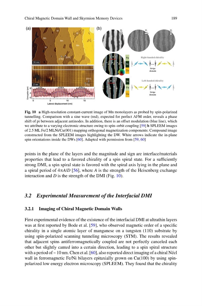
Fig. 10 a High-resolution constant-current image of Mn monolayers as probed by spin-polarized
tunnelling. Comparison with a sine wave (red), expected for perfect AFM order, reveals a phase
shift of pi between adjacent antinodes. In addition, there is an offset modulation (blue line), which
we attribute to a varying electronic structure owing to spin–orbit coupling [59] b SPLEEM images
of 2.5 ML Fe/2 MLNi/Cu(001) mapping orthogonal magnetization components: Compound image
constructed from the SPLEEM images highlighting the DW. White arrows indicate the in-plane
spin orientations inside the DWs [60]. Adapted with permission from [59, 60]
points in the plane of the layers and the magnitude and sign are interface/materials
properties that lead to a favored chirality of a spin spiral state. For a sufficiently
strong DMI, a spin spiral state is favored with the spiral axis lying in the plane and
a spiral period of 4πA/D [56], where A is the strength of the Heisenberg exchange
interaction and D is the strength of the DMI (Fig. 10).
3.2 Experimental Measurement of the Interfacial DMI
3.2.1 Imaging of Chiral Magnetic Domain Walls
First experimental evidence of the existence of the interfacial DMI at ultrathin layers
was at first reported by Bode et al. [59], who observed magnetic order of a specific
chirality in a single atomic layer of manganese on a tungsten (110) substrate by
using spin-polarized scanning tunneling microscopy (STM). The results revealed
that adjacent spins antiferromagnetically coupled are not perfectly canceled each
other but slightly canted into a certain direction, leading to a spin spiral structure
with a period of ~ 10 nm. Chen et al. [60], also reported direct imaging of a chiral Néel
wall in ferromagnetic Fe/Ni bilayers epitaxially grown on Cu(100) by using spinpolarized low energy electron microscopy (SPLEEM). They found that the chirality
189
Fig. 10 a High-resolution constant-current image of Mn monolayers as probed by spin-polarized
tunnelling. Comparison with a sine wave (red), expected for perfect AFM order, reveals a phase
shift of pi between adjacent antinodes. In addition, there is an offset modulation (blue line), which
we attribute to a varying electronic structure owing to spin–orbit coupling [59] b SPLEEM images
of 2.5 ML Fe/2 MLNi/Cu(001) mapping orthogonal magnetization components: Compound image
constructed from the SPLEEM images highlighting the DW. White arrows indicate the in-plane
spin orientations inside the DWs [60]. Adapted with permission from [59, 60]
points in the plane of the layers and the magnitude and sign are interface/materials
properties that lead to a favored chirality of a spin spiral state. For a sufficiently
strong DMI, a spin spiral state is favored with the spiral axis lying in the plane and
a spiral period of 4πA/D [56], where A is the strength of the Heisenberg exchange
interaction and D is the strength of the DMI (Fig. 10).
3.2 Experimental Measurement of the Interfacial DMI
3.2.1 Imaging of Chiral Magnetic Domain Walls
First experimental evidence of the existence of the interfacial DMI at ultrathin layers
was at first reported by Bode et al. [59], who observed magnetic order of a specific
chirality in a single atomic layer of manganese on a tungsten (110) substrate by
using spin-polarized scanning tunneling microscopy (STM). The results revealed
that adjacent spins antiferromagnetically coupled are not perfectly canceled each
other but slightly canted into a certain direction, leading to a spin spiral structure
with a period of ~ 10 nm. Chen et al. [60], also reported direct imaging of a chiral Néel
wall in ferromagnetic Fe/Ni bilayers epitaxially grown on Cu(100) by using spinpolarized low energy electron microscopy (SPLEEM). They found that the chirality