

166
J. Lourembam and J. Huang
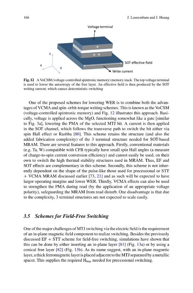
Fig. 12 A VoCSM (voltage-controlled spintronic memory) memory stack. The top voltage terminal
is used to lower the anisotropy of the free layer. An effective field is then produced by the SOT
writing current, which causes deterministic switching
One of the proposed schemes for lowering WER is to combine both the advantages of VCMA and spin–orbit-torque writing schemes. This is known as the VoCSM
(voltage-controlled spintronic memory) and Fig. 12 illustrates this approach. Basically, voltage is applied across the MgO, functioning somewhat like a gate [similar
to Fig. 3a], lowering the PMA of the selected MTJ bit. A current is then applied
in the SOT channel, which follows the transverse path to switch the bit either via
spin Hall effect or Rashba [80]. This scheme retains the structure (and also the
added fabrication complexity) of the 3 terminal structure needed for SOT-based
MRAM. There are several features to this approach. Firstly, conventional materials
(e.g. Ta, W) compatible with CFB typically have small spin Hall angles (a measure
of charge-to-spin current conversion efficiency) and cannot easily be used, on their
own to switch the high thermal stability structures used in MRAM. Thus, EF and
SOT effects are complementary in this scheme. Secondly, this scheme is not inherently dependent on the shape of the pulse-like those used for precessional or STT
+ VCMA MRAM discussed earlier [73, 21] and as such will be expected to have
larger operating margins and lower WER. Thirdly, VCMA effects can also be used
to strengthen the PMA during read (by the application of an appropriate voltage
polarity), safeguarding the MRAM from read disturb. One disadvantage is that due
to the complexity, 3 terminal structures are not expected to scale easily.
3.5 Schemes for Field-Free Switching
One of the major challenges of MTJ switching via the electric field is the requirement
of an in-plane magnetic field component to realize switching. Besides the previously
discussed EF + STT scheme for field-free switching, simulations have shown that
this can be done by either inserting an in-plane layer [81] (Fig. 13a) or by using a
conical free layer [82] (Fig. 13b). As its name suggest, with an in-plane magnetic
layer, a thick ferromagnetic layer is placed adjacent to the MTJ separated by a metallic
spacer. This supplies the required H bias needed for precessional switching.
J. Lourembam and J. Huang
Fig. 12 A VoCSM (voltage-controlled spintronic memory) memory stack. The top voltage terminal
is used to lower the anisotropy of the free layer. An effective field is then produced by the SOT
writing current, which causes deterministic switching
One of the proposed schemes for lowering WER is to combine both the advantages of VCMA and spin–orbit-torque writing schemes. This is known as the VoCSM
(voltage-controlled spintronic memory) and Fig. 12 illustrates this approach. Basically, voltage is applied across the MgO, functioning somewhat like a gate [similar
to Fig. 3a], lowering the PMA of the selected MTJ bit. A current is then applied
in the SOT channel, which follows the transverse path to switch the bit either via
spin Hall effect or Rashba [80]. This scheme retains the structure (and also the
added fabrication complexity) of the 3 terminal structure needed for SOT-based
MRAM. There are several features to this approach. Firstly, conventional materials
(e.g. Ta, W) compatible with CFB typically have small spin Hall angles (a measure
of charge-to-spin current conversion efficiency) and cannot easily be used, on their
own to switch the high thermal stability structures used in MRAM. Thus, EF and
SOT effects are complementary in this scheme. Secondly, this scheme is not inherently dependent on the shape of the pulse-like those used for precessional or STT
+ VCMA MRAM discussed earlier [73, 21] and as such will be expected to have
larger operating margins and lower WER. Thirdly, VCMA effects can also be used
to strengthen the PMA during read (by the application of an appropriate voltage
polarity), safeguarding the MRAM from read disturb. One disadvantage is that due
to the complexity, 3 terminal structures are not expected to scale easily.
3.5 Schemes for Field-Free Switching
One of the major challenges of MTJ switching via the electric field is the requirement
of an in-plane magnetic field component to realize switching. Besides the previously
discussed EF + STT scheme for field-free switching, simulations have shown that
this can be done by either inserting an in-plane layer [81] (Fig. 13a) or by using a
conical free layer [82] (Fig. 13b). As its name suggest, with an in-plane magnetic
layer, a thick ferromagnetic layer is placed adjacent to the MTJ separated by a metallic
spacer. This supplies the required H bias needed for precessional switching.