

Electric-Field-Controlled MRAM: Physics and Applications
165
or tighter than the current pulses used in STT-MRAM [76]. However, even with
moderate increases in temperature (room to 50 °C), the WER increases significantly
from 10
−8 to 10
−4 [76]. The authors attributed this to the reduction in magnetization,
which reduces the in-plane demagnetization field. This causes an increase in the
Larmor frequency when the same pulse amplitude is used. While this can be solved
with various circuit workarounds like pre-reads (writing only if the bit is in the wrong
state) and the multiple writes (correcting for bits that fail to write correctly on the
first pulse), this poses a challenge since consumer specs require a range of at least 0
to 70 °C [74].
Unlike conventional CMOS-based memory, MRAM is inherently probabilistic
due to the thermal energy barrier. For STT-MRAM, one can increase write pulse
widths such that one is always writing in the thermal activation regime. This brings
the BER down to levels that can be covered by ECC [77]. However, for E-field
MRAM schemes that use precessional switching primarily, the narrow pulse width
switching windows make designs difficult without additional circuit workarounds.
As shown by the switching probably in Fig. 8c, It can be seen that the switching
probability drops drastically, the further the pulse width is away from the peak. The
switching error rate of a single bit has been further experimentally studied by Shiota
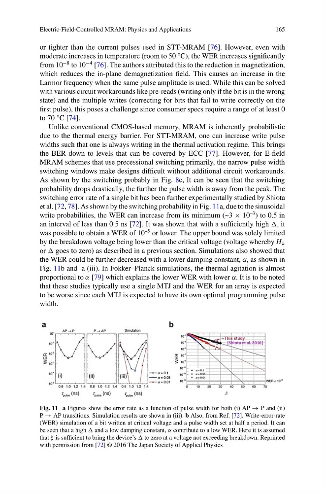
et al. [72, 78]. As shown by the switching probability in Fig. 11a, due to the sinusoidal
write probabilities, the WER can increase from its minimum (~3 × 10
–3 ) to 0.5 in
an interval of less than 0.5 ns [72]. It was shown that with a sufficiently high , it
was possible to obtain a WER of 10
–5 or lower. The upper bound was solely limited
by the breakdown voltage being lower than the critical voltage (voltage whereby H k
or goes to zero) as described in a previous section. Simulations also showed that
the WER could be further decreased with a lower damping constant, α, as shown in
Fig. 11b and a (iii). In Fokker–Planck simulations, the thermal agitation is almost
proportional to α [79] which explains the lower WER with lower α. It is to be noted
that these studies typically use a single MTJ and the WER for an array is expected
to be worse since each MTJ is expected to have its own optimal programming pulse
width.
Fig. 11 a Figures show the error rate as a function of pulse width for both (i) AP → P and (ii)
P → AP transitions. Simulation results are shown in (iii). b Also, from Ref. [72]. Write-error-rate
(WER) simulation of a bit written at critical voltage and a pulse width set at half a period. It can
be seen that a high and a low damping constant, α contribute to a low WER. Here it is assumed
that ξ is sufficient to bring the device’s to zero at a voltage not exceeding breakdown. Reprinted
with permission from [72] © 2016 The Japan Society of Applied Physics
165
or tighter than the current pulses used in STT-MRAM [76]. However, even with
moderate increases in temperature (room to 50 °C), the WER increases significantly
from 10
−8 to 10
−4 [76]. The authors attributed this to the reduction in magnetization,
which reduces the in-plane demagnetization field. This causes an increase in the
Larmor frequency when the same pulse amplitude is used. While this can be solved
with various circuit workarounds like pre-reads (writing only if the bit is in the wrong
state) and the multiple writes (correcting for bits that fail to write correctly on the
first pulse), this poses a challenge since consumer specs require a range of at least 0
to 70 °C [74].
Unlike conventional CMOS-based memory, MRAM is inherently probabilistic
due to the thermal energy barrier. For STT-MRAM, one can increase write pulse
widths such that one is always writing in the thermal activation regime. This brings
the BER down to levels that can be covered by ECC [77]. However, for E-field
MRAM schemes that use precessional switching primarily, the narrow pulse width
switching windows make designs difficult without additional circuit workarounds.
As shown by the switching probably in Fig. 8c, It can be seen that the switching
probability drops drastically, the further the pulse width is away from the peak. The
switching error rate of a single bit has been further experimentally studied by Shiota
et al. [72, 78]. As shown by the switching probability in Fig. 11a, due to the sinusoidal
write probabilities, the WER can increase from its minimum (~3 × 10
–3 ) to 0.5 in
an interval of less than 0.5 ns [72]. It was shown that with a sufficiently high , it
was possible to obtain a WER of 10
–5 or lower. The upper bound was solely limited
by the breakdown voltage being lower than the critical voltage (voltage whereby H k
or goes to zero) as described in a previous section. Simulations also showed that
the WER could be further decreased with a lower damping constant, α, as shown in
Fig. 11b and a (iii). In Fokker–Planck simulations, the thermal agitation is almost
proportional to α [79] which explains the lower WER with lower α. It is to be noted
that these studies typically use a single MTJ and the WER for an array is expected
to be worse since each MTJ is expected to have its own optimal programming pulse
width.
Fig. 11 a Figures show the error rate as a function of pulse width for both (i) AP → P and (ii)
P → AP transitions. Simulation results are shown in (iii). b Also, from Ref. [72]. Write-error-rate
(WER) simulation of a bit written at critical voltage and a pulse width set at half a period. It can
be seen that a high and a low damping constant, α contribute to a low WER. Here it is assumed
that ξ is sufficient to bring the device’s to zero at a voltage not exceeding breakdown. Reprinted
with permission from [72] © 2016 The Japan Society of Applied Physics