

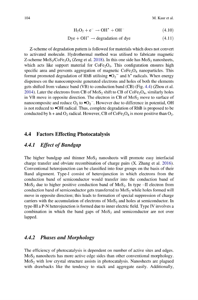
H 2 O 2 þ e
À
! OH
•
þ OH
À
ð4:10Þ
Dye þ OH
•
! degradation of dye
ð4:11Þ
Z-scheme of degradation pattern is followed for materials which does not convert
to activated molecule. Hydrothermal method was utilised to fabricate magnetic
Z-scheme MoS 2 /CoFe 2 O 4 (Zeng et al. 2018). In this one side has MoS 2 nanosheets,
which acts like support material for CoFe 2 O 4 . This configuration ensures high
specific area and prevents aggregation of magnetic CoFe 2 O 4 nanoparticles. This
format promoted degradation of RhB utilising ⦁O 2
À and h
+ radicals. When energy
dispenses on the nanocomposite generated electrons and holes of both the elements
gets shifted from valance band (VB) to conduction band (CB) (Fig. 4.4) (Zhou et al.
2014). Later the electrons from CB of MoS 2 shift to CB of CoFe 2 O 4 , similarly holes
in VB move in opposite direction. The electron in CB of MoS 2 move to surface of
nanocomposite and reduce O 2 to ⦁O 2
À . However due to difference in potential, OH
is not reduced to ⦁OH radical. Thus, complete degradation of RhB is proposed to be
conducted by h + and O 2 radical. However, CB of CoFe 2 O 4 is more positive than O 2 .
4.4 Factors Effecting Photocatalysis
4.4.1 Effect of Bandgap
The higher bandgap and thinner MoS 2 nanosheets will promote easy interfacial
charge transfer and obviate recombination of charge pairs (X. Zhang et al. 2016).
Conventional heterojunction can be classified into four groups on the basis of their
Band alignment. Type-I consist of heterojunction in which electrons from the
conduction band of semiconductor would transfer into the conduction band of
MoS 2 due to higher positive conduction band of MoS 2 . In type –II electron from
conduction band of semiconductor gets transferred to MoS 2 while holes formed will
move in opposite direction; this leads to formation of special suppression of charge
carriers with the accumulation of electrons of MoS 2 and holes at semiconductor. In
type-III a P-N heterojunction is formed due to inner electric field. Type IV involves a
combination in which the band gaps of MoS 2 and semiconductor are not over
lapped.
4.4.2 Phases and Morphology
The efficiency of photocatalysis is dependent on number of active sites and edges.
MoS 2 nanosheets has more active edge sides than other conventional morphology.
MoS 2 with low crystal structure assists in photocatalysis. Nanosheets are plagued
with drawbacks like the tendency to stack and aggregate easily. Additionally,
104
M. Kaur et al.
À
! OH
•
þ OH
À
ð4:10Þ
Dye þ OH
•
! degradation of dye
ð4:11Þ
Z-scheme of degradation pattern is followed for materials which does not convert
to activated molecule. Hydrothermal method was utilised to fabricate magnetic
Z-scheme MoS 2 /CoFe 2 O 4 (Zeng et al. 2018). In this one side has MoS 2 nanosheets,
which acts like support material for CoFe 2 O 4 . This configuration ensures high
specific area and prevents aggregation of magnetic CoFe 2 O 4 nanoparticles. This
format promoted degradation of RhB utilising ⦁O 2
À and h
+ radicals. When energy
dispenses on the nanocomposite generated electrons and holes of both the elements
gets shifted from valance band (VB) to conduction band (CB) (Fig. 4.4) (Zhou et al.
2014). Later the electrons from CB of MoS 2 shift to CB of CoFe 2 O 4 , similarly holes
in VB move in opposite direction. The electron in CB of MoS 2 move to surface of
nanocomposite and reduce O 2 to ⦁O 2
À . However due to difference in potential, OH
is not reduced to ⦁OH radical. Thus, complete degradation of RhB is proposed to be
conducted by h + and O 2 radical. However, CB of CoFe 2 O 4 is more positive than O 2 .
4.4 Factors Effecting Photocatalysis
4.4.1 Effect of Bandgap
The higher bandgap and thinner MoS 2 nanosheets will promote easy interfacial
charge transfer and obviate recombination of charge pairs (X. Zhang et al. 2016).
Conventional heterojunction can be classified into four groups on the basis of their
Band alignment. Type-I consist of heterojunction in which electrons from the
conduction band of semiconductor would transfer into the conduction band of
MoS 2 due to higher positive conduction band of MoS 2 . In type –II electron from
conduction band of semiconductor gets transferred to MoS 2 while holes formed will
move in opposite direction; this leads to formation of special suppression of charge
carriers with the accumulation of electrons of MoS 2 and holes at semiconductor. In
type-III a P-N heterojunction is formed due to inner electric field. Type IV involves a
combination in which the band gaps of MoS 2 and semiconductor are not over
lapped.
4.4.2 Phases and Morphology
The efficiency of photocatalysis is dependent on number of active sites and edges.
MoS 2 nanosheets has more active edge sides than other conventional morphology.
MoS 2 with low crystal structure assists in photocatalysis. Nanosheets are plagued
with drawbacks like the tendency to stack and aggregate easily. Additionally,
104
M. Kaur et al.