

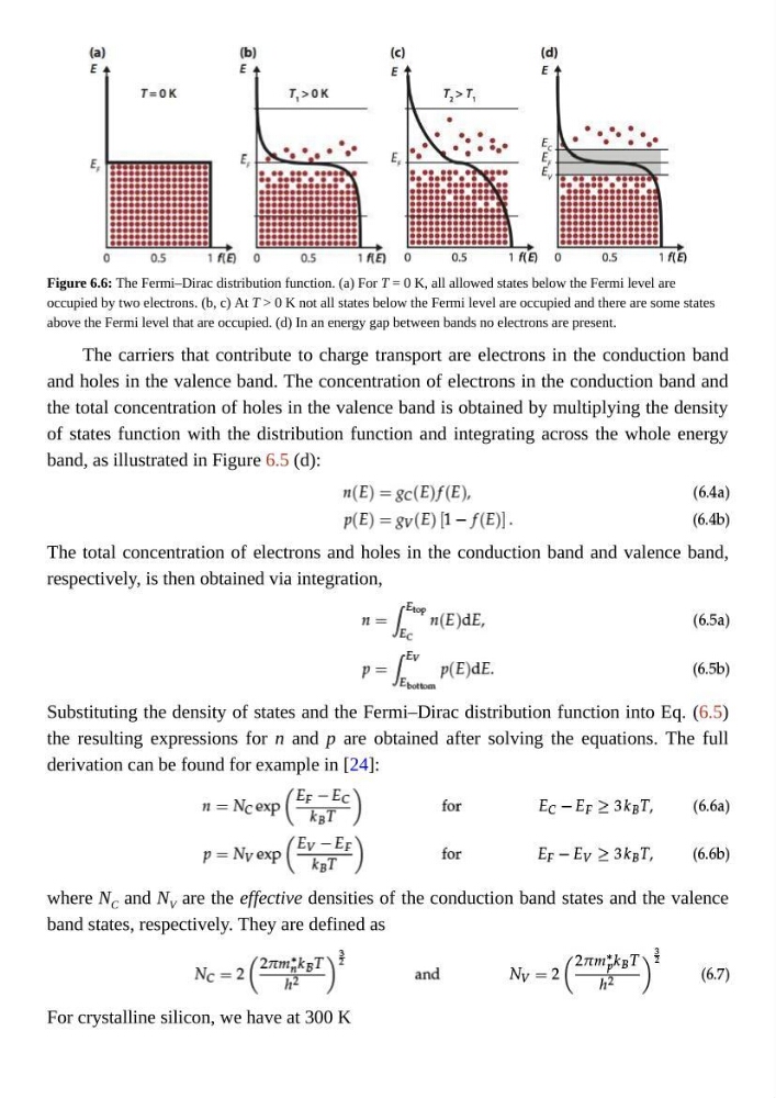
Figure 6.6: The Fermi–Dirac distribution function. (a) For T = 0 K, all allowed states below the Fermi level are
occupied by two electrons. (b, c) At T > 0 K not all states below the Fermi level are occupied and there are some states
above the Fermi level that are occupied. (d) In an energy gap between bands no electrons are present.
The carriers that contribute to charge transport are electrons in the conduction band
and holes in the valence band. The concentration of electrons in the conduction band and
the total concentration of holes in the valence band is obtained by multiplying the density
of states function with the distribution function and integrating across the whole energy
band, as illustrated in Figure 6.5 (d):
The total concentration of electrons and holes in the conduction band and valence band,
respectively, is then obtained via integration,
Substituting the density of states and the Fermi–Dirac distribution function into Eq. (6.5)
the resulting expressions for n and p are obtained after solving the equations. The full
derivation can be found for example in [24]:
where N C and N V are the effective densities of the conduction band states and the valence
band states, respectively. They are defined as
For crystalline silicon, we have at 300 K
occupied by two electrons. (b, c) At T > 0 K not all states below the Fermi level are occupied and there are some states
above the Fermi level that are occupied. (d) In an energy gap between bands no electrons are present.
The carriers that contribute to charge transport are electrons in the conduction band
and holes in the valence band. The concentration of electrons in the conduction band and
the total concentration of holes in the valence band is obtained by multiplying the density
of states function with the distribution function and integrating across the whole energy
band, as illustrated in Figure 6.5 (d):
The total concentration of electrons and holes in the conduction band and valence band,
respectively, is then obtained via integration,
Substituting the density of states and the Fermi–Dirac distribution function into Eq. (6.5)
the resulting expressions for n and p are obtained after solving the equations. The full
derivation can be found for example in [24]:
where N C and N V are the effective densities of the conduction band states and the valence
band states, respectively. They are defined as
For crystalline silicon, we have at 300 K