

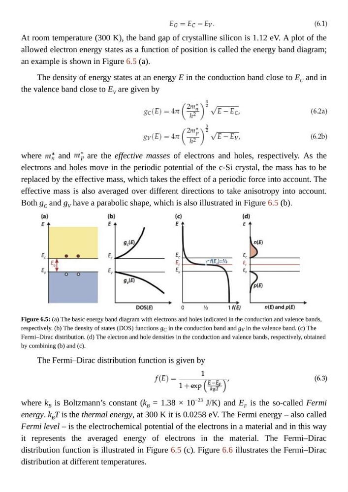
At room temperature (300 K), the band gap of crystalline silicon is 1.12 eV. A plot of the
allowed electron energy states as a function of position is called the energy band diagram;
an example is shown in Figure 6.5 (a).
The density of energy states at an energy E in the conduction band close to E C and in
the valence band close to E V are given by
where and are the effective masses of electrons and holes, respectively. As the
electrons and holes move in the periodic potential of the c-Si crystal, the mass has to be
replaced by the effective mass, which takes the effect of a periodic force into account. The
effective mass is also averaged over different directions to take anisotropy into account.
Both g C and g V have a parabolic shape, which is also illustrated in Figure 6.5 (b).
Figure 6.5: (a) The basic energy band diagram with electrons and holes indicated in the conduction and valence bands,
respectively. (b) The density of states (DOS) functions g C in the conduction band and g V in the valence band. (c) The
Fermi–Dirac distribution. (d) The electron and hole densities in the conduction and valence bands, respectively, obtained
by combining (b) and (c).
The Fermi–Dirac distribution function is given by
where k B is Boltzmann’s constant (k B = 1.38 × 10
−23
J/K) and E F is the so-called Fermi
energy. k B T is the thermal energy, at 300 K it is 0.0258 eV. The Fermi energy – also called
Fermi level – is the electrochemical potential of the electrons in a material and in this way
it represents the averaged energy of electrons in the material. The Fermi–Dirac
distribution function is illustrated in Figure 6.5 (c). Figure 6.6 illustrates the Fermi–Dirac
distribution at different temperatures.
allowed electron energy states as a function of position is called the energy band diagram;
an example is shown in Figure 6.5 (a).
The density of energy states at an energy E in the conduction band close to E C and in
the valence band close to E V are given by
where and are the effective masses of electrons and holes, respectively. As the
electrons and holes move in the periodic potential of the c-Si crystal, the mass has to be
replaced by the effective mass, which takes the effect of a periodic force into account. The
effective mass is also averaged over different directions to take anisotropy into account.
Both g C and g V have a parabolic shape, which is also illustrated in Figure 6.5 (b).
Figure 6.5: (a) The basic energy band diagram with electrons and holes indicated in the conduction and valence bands,
respectively. (b) The density of states (DOS) functions g C in the conduction band and g V in the valence band. (c) The
Fermi–Dirac distribution. (d) The electron and hole densities in the conduction and valence bands, respectively, obtained
by combining (b) and (c).
The Fermi–Dirac distribution function is given by
where k B is Boltzmann’s constant (k B = 1.38 × 10
−23
J/K) and E F is the so-called Fermi
energy. k B T is the thermal energy, at 300 K it is 0.0258 eV. The Fermi energy – also called
Fermi level – is the electrochemical potential of the electrons in a material and in this way
it represents the averaged energy of electrons in the material. The Fermi–Dirac
distribution function is illustrated in Figure 6.5 (c). Figure 6.6 illustrates the Fermi–Dirac
distribution at different temperatures.