

6.4
6.4.1
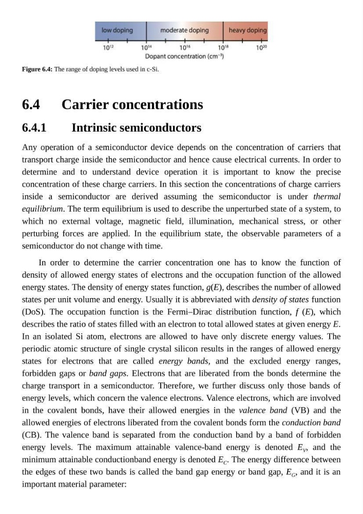
Figure 6.4: The range of doping levels used in c-Si.
Carrier concentrations
Intrinsic semiconductors
Any operation of a semiconductor device depends on the concentration of carriers that
transport charge inside the semiconductor and hence cause electrical currents. In order to
determine and to understand device operation it is important to know the precise
concentration of these charge carriers. In this section the concentrations of charge carriers
inside a semiconductor are derived assuming the semiconductor is under thermal
equilibrium. The term equilibrium is used to describe the unperturbed state of a system, to
which no external voltage, magnetic field, illumination, mechanical stress, or other
perturbing forces are applied. In the equilibrium state, the observable parameters of a
semiconductor do not change with time.
In order to determine the carrier concentration one has to know the function of
density of allowed energy states of electrons and the occupation function of the allowed
energy states. The density of energy states function, g(E), describes the number of allowed
states per unit volume and energy. Usually it is abbreviated with density of states function
(DoS). The occupation function is the Fermi–Dirac distribution function, f (E), which
describes the ratio of states filled with an electron to total allowed states at given energy E.
In an isolated Si atom, electrons are allowed to have only discrete energy values. The
periodic atomic structure of single crystal silicon results in the ranges of allowed energy
states for electrons that are called energy bands, and the excluded energy ranges,
forbidden gaps or band gaps. Electrons that are liberated from the bonds determine the
charge transport in a semiconductor. Therefore, we further discuss only those bands of
energy levels, which concern the valence electrons. Valence electrons, which are involved
in the covalent bonds, have their allowed energies in the valence band (VB) and the
allowed energies of electrons liberated from the covalent bonds form the conduction band
(CB). The valence band is separated from the conduction band by a band of forbidden
energy levels. The maximum attainable valence-band energy is denoted E V , and the
minimum attainable conductionband energy is denoted E C . The energy difference between
the edges of these two bands is called the band gap energy or band gap, E G , and it is an
important material parameter:
6.4.1
Figure 6.4: The range of doping levels used in c-Si.
Carrier concentrations
Intrinsic semiconductors
Any operation of a semiconductor device depends on the concentration of carriers that
transport charge inside the semiconductor and hence cause electrical currents. In order to
determine and to understand device operation it is important to know the precise
concentration of these charge carriers. In this section the concentrations of charge carriers
inside a semiconductor are derived assuming the semiconductor is under thermal
equilibrium. The term equilibrium is used to describe the unperturbed state of a system, to
which no external voltage, magnetic field, illumination, mechanical stress, or other
perturbing forces are applied. In the equilibrium state, the observable parameters of a
semiconductor do not change with time.
In order to determine the carrier concentration one has to know the function of
density of allowed energy states of electrons and the occupation function of the allowed
energy states. The density of energy states function, g(E), describes the number of allowed
states per unit volume and energy. Usually it is abbreviated with density of states function
(DoS). The occupation function is the Fermi–Dirac distribution function, f (E), which
describes the ratio of states filled with an electron to total allowed states at given energy E.
In an isolated Si atom, electrons are allowed to have only discrete energy values. The
periodic atomic structure of single crystal silicon results in the ranges of allowed energy
states for electrons that are called energy bands, and the excluded energy ranges,
forbidden gaps or band gaps. Electrons that are liberated from the bonds determine the
charge transport in a semiconductor. Therefore, we further discuss only those bands of
energy levels, which concern the valence electrons. Valence electrons, which are involved
in the covalent bonds, have their allowed energies in the valence band (VB) and the
allowed energies of electrons liberated from the covalent bonds form the conduction band
(CB). The valence band is separated from the conduction band by a band of forbidden
energy levels. The maximum attainable valence-band energy is denoted E V , and the
minimum attainable conductionband energy is denoted E C . The energy difference between
the edges of these two bands is called the band gap energy or band gap, E G , and it is an
important material parameter: