

13.3.2
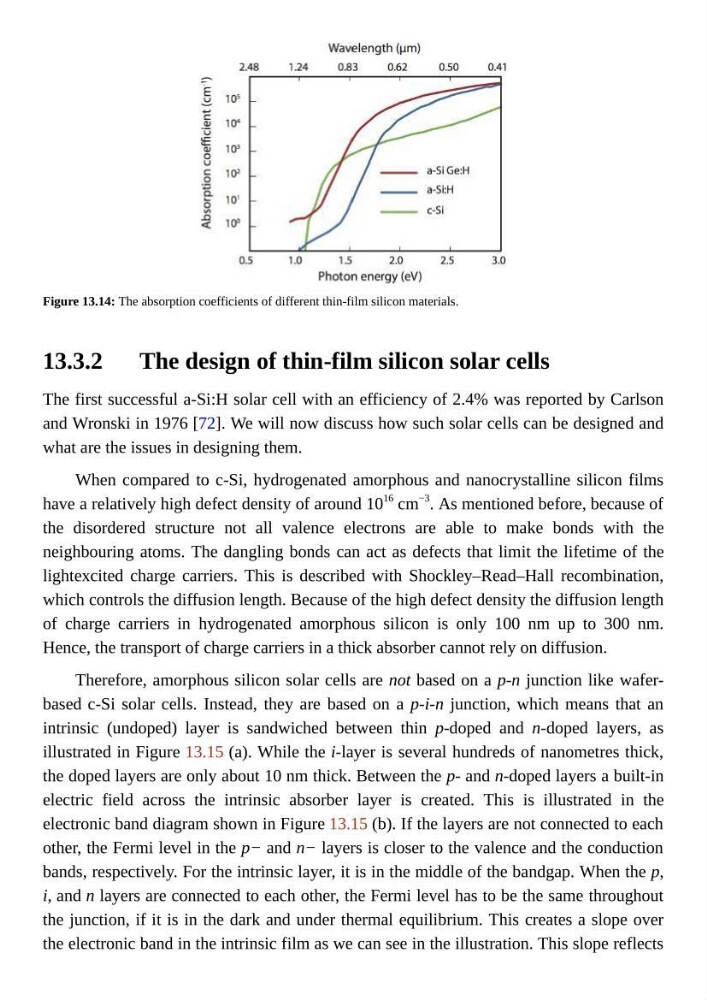
Figure 13.14: The absorption coefficients of different thin-film silicon materials.
The design of thin-film silicon solar cells
The first successful a-Si:H solar cell with an efficiency of 2.4% was reported by Carlson
and Wronski in 1976 [72]. We will now discuss how such solar cells can be designed and
what are the issues in designing them.
When compared to c-Si, hydrogenated amorphous and nanocrystalline silicon films
have a relatively high defect density of around 10
16
cm
−3
. As mentioned before, because of
the disordered structure not all valence electrons are able to make bonds with the
neighbouring atoms. The dangling bonds can act as defects that limit the lifetime of the
lightexcited charge carriers. This is described with Shockley–Read–Hall recombination,
which controls the diffusion length. Because of the high defect density the diffusion length
of charge carriers in hydrogenated amorphous silicon is only 100 nm up to 300 nm.
Hence, the transport of charge carriers in a thick absorber cannot rely on diffusion.
Therefore, amorphous silicon solar cells are not based on a p-n junction like waferbased c-Si solar cells. Instead, they are based on a p-i-n junction, which means that an
intrinsic (undoped) layer is sandwiched between thin p-doped and n-doped layers, as
illustrated in Figure 13.15 (a). While the i-layer is several hundreds of nanometres thick,
the doped layers are only about 10 nm thick. Between the p- and n-doped layers a built-in
electric field across the intrinsic absorber layer is created. This is illustrated in the
electronic band diagram shown in Figure 13.15 (b). If the layers are not connected to each
other, the Fermi level in the p− and n− layers is closer to the valence and the conduction
bands, respectively. For the intrinsic layer, it is in the middle of the bandgap. When the p,
i, and n layers are connected to each other, the Fermi level has to be the same throughout
the junction, if it is in the dark and under thermal equilibrium. This creates a slope over
the electronic band in the intrinsic film as we can see in the illustration. This slope reflects
Figure 13.14: The absorption coefficients of different thin-film silicon materials.
The design of thin-film silicon solar cells
The first successful a-Si:H solar cell with an efficiency of 2.4% was reported by Carlson
and Wronski in 1976 [72]. We will now discuss how such solar cells can be designed and
what are the issues in designing them.
When compared to c-Si, hydrogenated amorphous and nanocrystalline silicon films
have a relatively high defect density of around 10
16
cm
−3
. As mentioned before, because of
the disordered structure not all valence electrons are able to make bonds with the
neighbouring atoms. The dangling bonds can act as defects that limit the lifetime of the
lightexcited charge carriers. This is described with Shockley–Read–Hall recombination,
which controls the diffusion length. Because of the high defect density the diffusion length
of charge carriers in hydrogenated amorphous silicon is only 100 nm up to 300 nm.
Hence, the transport of charge carriers in a thick absorber cannot rely on diffusion.
Therefore, amorphous silicon solar cells are not based on a p-n junction like waferbased c-Si solar cells. Instead, they are based on a p-i-n junction, which means that an
intrinsic (undoped) layer is sandwiched between thin p-doped and n-doped layers, as
illustrated in Figure 13.15 (a). While the i-layer is several hundreds of nanometres thick,
the doped layers are only about 10 nm thick. Between the p- and n-doped layers a built-in
electric field across the intrinsic absorber layer is created. This is illustrated in the
electronic band diagram shown in Figure 13.15 (b). If the layers are not connected to each
other, the Fermi level in the p− and n− layers is closer to the valence and the conduction
bands, respectively. For the intrinsic layer, it is in the middle of the bandgap. When the p,
i, and n layers are connected to each other, the Fermi level has to be the same throughout
the junction, if it is in the dark and under thermal equilibrium. This creates a slope over
the electronic band in the intrinsic film as we can see in the illustration. This slope reflects