

the built-in electric field.
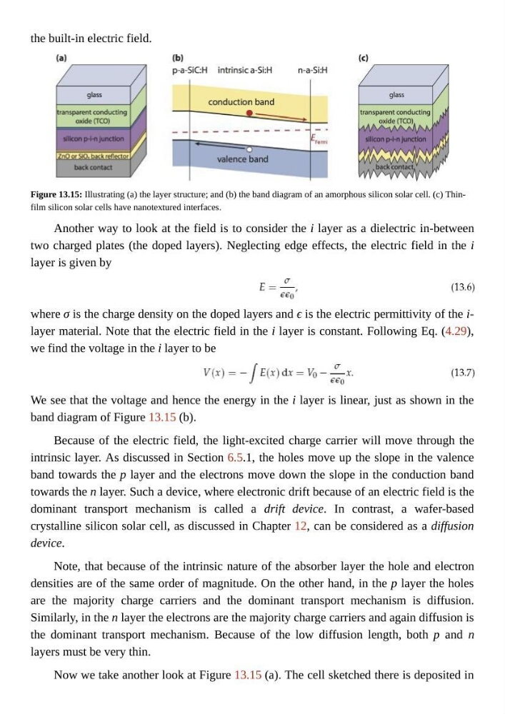
Figure 13.15: Illustrating (a) the layer structure; and (b) the band diagram of an amorphous silicon solar cell. (c) Thinfilm silicon solar cells have nanotextured interfaces.
Another way to look at the field is to consider the i layer as a dielectric in-between
two charged plates (the doped layers). Neglecting edge effects, the electric field in the i
layer is given by
where σ is the charge density on the doped layers and ϵ is the electric permittivity of the ilayer material. Note that the electric field in the i layer is constant. Following Eq. (4.29),
we find the voltage in the i layer to be
We see that the voltage and hence the energy in the i layer is linear, just as shown in the
band diagram of Figure 13.15 (b).
Because of the electric field, the light-excited charge carrier will move through the
intrinsic layer. As discussed in Section 6.5.1, the holes move up the slope in the valence
band towards the p layer and the electrons move down the slope in the conduction band
towards the n layer. Such a device, where electronic drift because of an electric field is the
dominant transport mechanism is called a drift device. In contrast, a wafer-based
crystalline silicon solar cell, as discussed in Chapter 12, can be considered as a diffusion
device.
Note, that because of the intrinsic nature of the absorber layer the hole and electron
densities are of the same order of magnitude. On the other hand, in the p layer the holes
are the majority charge carriers and the dominant transport mechanism is diffusion.
Similarly, in the n layer the electrons are the majority charge carriers and again diffusion is
the dominant transport mechanism. Because of the low diffusion length, both p and n
layers must be very thin.
Now we take another look at Figure 13.15 (a). The cell sketched there is deposited in
Figure 13.15: Illustrating (a) the layer structure; and (b) the band diagram of an amorphous silicon solar cell. (c) Thinfilm silicon solar cells have nanotextured interfaces.
Another way to look at the field is to consider the i layer as a dielectric in-between
two charged plates (the doped layers). Neglecting edge effects, the electric field in the i
layer is given by
where σ is the charge density on the doped layers and ϵ is the electric permittivity of the ilayer material. Note that the electric field in the i layer is constant. Following Eq. (4.29),
we find the voltage in the i layer to be
We see that the voltage and hence the energy in the i layer is linear, just as shown in the
band diagram of Figure 13.15 (b).
Because of the electric field, the light-excited charge carrier will move through the
intrinsic layer. As discussed in Section 6.5.1, the holes move up the slope in the valence
band towards the p layer and the electrons move down the slope in the conduction band
towards the n layer. Such a device, where electronic drift because of an electric field is the
dominant transport mechanism is called a drift device. In contrast, a wafer-based
crystalline silicon solar cell, as discussed in Chapter 12, can be considered as a diffusion
device.
Note, that because of the intrinsic nature of the absorber layer the hole and electron
densities are of the same order of magnitude. On the other hand, in the p layer the holes
are the majority charge carriers and the dominant transport mechanism is diffusion.
Similarly, in the n layer the electrons are the majority charge carriers and again diffusion is
the dominant transport mechanism. Because of the low diffusion length, both p and n
layers must be very thin.
Now we take another look at Figure 13.15 (a). The cell sketched there is deposited in