

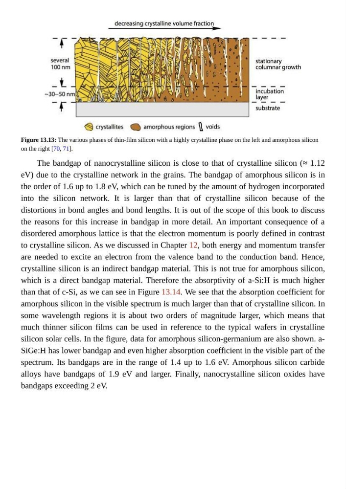
Figure 13.13: The various phases of thin-film silicon with a highly crystalline phase on the left and amorphous silicon
on the right [70, 71].
The bandgap of nanocrystalline silicon is close to that of crystalline silicon (≈ 1.12
eV) due to the crystalline network in the grains. The bandgap of amorphous silicon is in
the order of 1.6 up to 1.8 eV, which can be tuned by the amount of hydrogen incorporated
into the silicon network. It is larger than that of crystalline silicon because of the
distortions in bond angles and bond lengths. It is out of the scope of this book to discuss
the reasons for this increase in bandgap in more detail. An important consequence of a
disordered amorphous lattice is that the electron momentum is poorly defined in contrast
to crystalline silicon. As we discussed in Chapter 12, both energy and momentum transfer
are needed to excite an electron from the valence band to the conduction band. Hence,
crystalline silicon is an indirect bandgap material. This is not true for amorphous silicon,
which is a direct bandgap material. Therefore the absorptivity of a-Si:H is much higher
than that of c-Si, as we can see in Figure 13.14. We see that the absorption coefficient for
amorphous silicon in the visible spectrum is much larger than that of crystalline silicon. In
some wavelength regions it is about two orders of magnitude larger, which means that
much thinner silicon films can be used in reference to the typical wafers in crystalline
silicon solar cells. In the figure, data for amorphous silicon-germanium are also shown. aSiGe:H has lower bandgap and even higher absorption coefficient in the visible part of the
spectrum. Its bandgaps are in the range of 1.4 up to 1.6 eV. Amorphous silicon carbide
alloys have bandgaps of 1.9 eV and larger. Finally, nanocrystalline silicon oxides have
bandgaps exceeding 2 eV.
on the right [70, 71].
The bandgap of nanocrystalline silicon is close to that of crystalline silicon (≈ 1.12
eV) due to the crystalline network in the grains. The bandgap of amorphous silicon is in
the order of 1.6 up to 1.8 eV, which can be tuned by the amount of hydrogen incorporated
into the silicon network. It is larger than that of crystalline silicon because of the
distortions in bond angles and bond lengths. It is out of the scope of this book to discuss
the reasons for this increase in bandgap in more detail. An important consequence of a
disordered amorphous lattice is that the electron momentum is poorly defined in contrast
to crystalline silicon. As we discussed in Chapter 12, both energy and momentum transfer
are needed to excite an electron from the valence band to the conduction band. Hence,
crystalline silicon is an indirect bandgap material. This is not true for amorphous silicon,
which is a direct bandgap material. Therefore the absorptivity of a-Si:H is much higher
than that of c-Si, as we can see in Figure 13.14. We see that the absorption coefficient for
amorphous silicon in the visible spectrum is much larger than that of crystalline silicon. In
some wavelength regions it is about two orders of magnitude larger, which means that
much thinner silicon films can be used in reference to the typical wafers in crystalline
silicon solar cells. In the figure, data for amorphous silicon-germanium are also shown. aSiGe:H has lower bandgap and even higher absorption coefficient in the visible part of the
spectrum. Its bandgaps are in the range of 1.4 up to 1.6 eV. Amorphous silicon carbide
alloys have bandgaps of 1.9 eV and larger. Finally, nanocrystalline silicon oxides have
bandgaps exceeding 2 eV.