

junctions in series, for example the p-layer of the top cell and the n-layer of the middle
cell would form a p-n junction in the reverse direction than the p-n junctions of the three
single-junction solar cells. These reverse junctions would significantly lower the voltage
of the total triple junction.
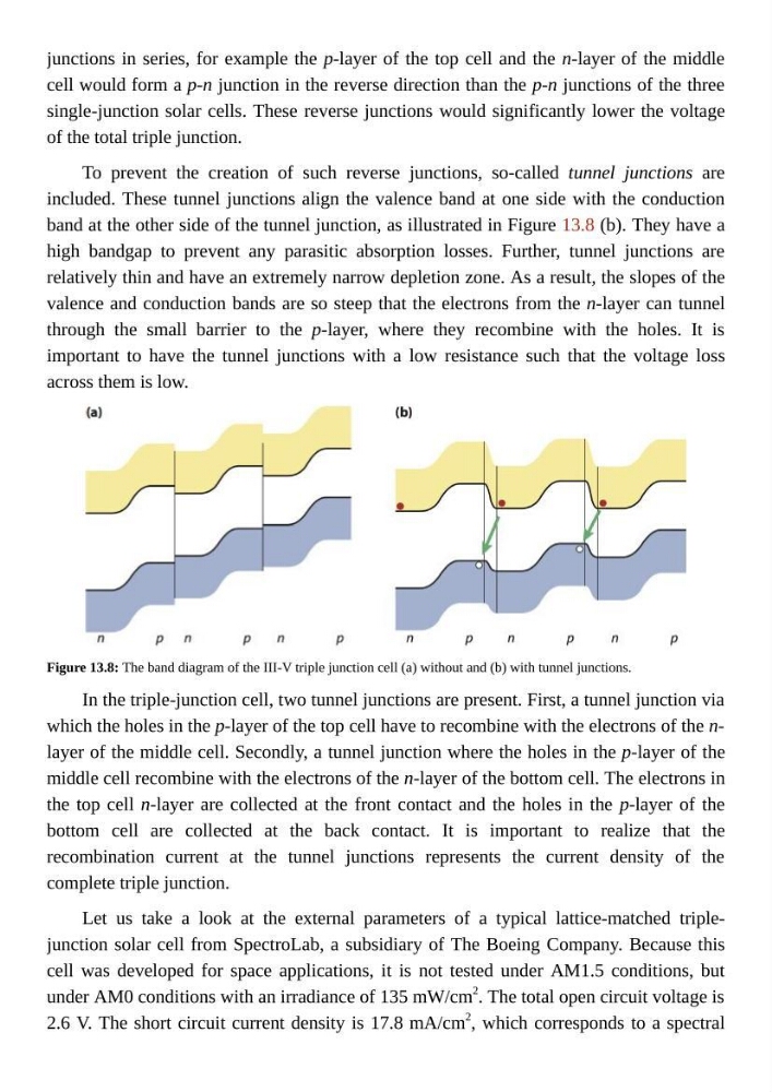
To prevent the creation of such reverse junctions, so-called tunnel junctions are
included. These tunnel junctions align the valence band at one side with the conduction
band at the other side of the tunnel junction, as illustrated in Figure 13.8 (b). They have a
high bandgap to prevent any parasitic absorption losses. Further, tunnel junctions are
relatively thin and have an extremely narrow depletion zone. As a result, the slopes of the
valence and conduction bands are so steep that the electrons from the n-layer can tunnel
through the small barrier to the p-layer, where they recombine with the holes. It is
important to have the tunnel junctions with a low resistance such that the voltage loss
across them is low.
Figure 13.8: The band diagram of the III-V triple junction cell (a) without and (b) with tunnel junctions.
In the triple-junction cell, two tunnel junctions are present. First, a tunnel junction via
which the holes in the p-layer of the top cell have to recombine with the electrons of the nlayer of the middle cell. Secondly, a tunnel junction where the holes in the p-layer of the
middle cell recombine with the electrons of the n-layer of the bottom cell. The electrons in
the top cell n-layer are collected at the front contact and the holes in the p-layer of the
bottom cell are collected at the back contact. It is important to realize that the
recombination current at the tunnel junctions represents the current density of the
complete triple junction.
Let us take a look at the external parameters of a typical lattice-matched triplejunction solar cell from SpectroLab, a subsidiary of The Boeing Company. Because this
cell was developed for space applications, it is not tested under AM1.5 conditions, but
under AM0 conditions with an irradiance of 135 mW/cm
2
. The total open circuit voltage is
2.6 V. The short circuit current density is 17.8 mA/cm
2 , which corresponds to a spectral
cell would form a p-n junction in the reverse direction than the p-n junctions of the three
single-junction solar cells. These reverse junctions would significantly lower the voltage
of the total triple junction.
To prevent the creation of such reverse junctions, so-called tunnel junctions are
included. These tunnel junctions align the valence band at one side with the conduction
band at the other side of the tunnel junction, as illustrated in Figure 13.8 (b). They have a
high bandgap to prevent any parasitic absorption losses. Further, tunnel junctions are
relatively thin and have an extremely narrow depletion zone. As a result, the slopes of the
valence and conduction bands are so steep that the electrons from the n-layer can tunnel
through the small barrier to the p-layer, where they recombine with the holes. It is
important to have the tunnel junctions with a low resistance such that the voltage loss
across them is low.
Figure 13.8: The band diagram of the III-V triple junction cell (a) without and (b) with tunnel junctions.
In the triple-junction cell, two tunnel junctions are present. First, a tunnel junction via
which the holes in the p-layer of the top cell have to recombine with the electrons of the nlayer of the middle cell. Secondly, a tunnel junction where the holes in the p-layer of the
middle cell recombine with the electrons of the n-layer of the bottom cell. The electrons in
the top cell n-layer are collected at the front contact and the holes in the p-layer of the
bottom cell are collected at the back contact. It is important to realize that the
recombination current at the tunnel junctions represents the current density of the
complete triple junction.
Let us take a look at the external parameters of a typical lattice-matched triplejunction solar cell from SpectroLab, a subsidiary of The Boeing Company. Because this
cell was developed for space applications, it is not tested under AM1.5 conditions, but
under AM0 conditions with an irradiance of 135 mW/cm
2
. The total open circuit voltage is
2.6 V. The short circuit current density is 17.8 mA/cm
2 , which corresponds to a spectral