

12.4
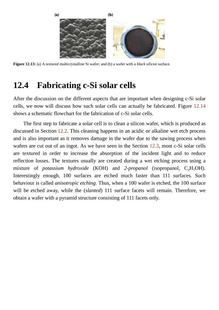
Figure 12.13: (a) A textured multicrystalline Si wafer; and (b) a wafer with a black silicon surface.
Fabricating c-Si solar cells
After the discussion on the different aspects that are important when designing c-Si solar
cells, we now will discuss how such solar cells can actually be fabricated. Figure 12.14
shows a schematic flowchart for the fabrication of c-Si solar cells.
The first step to fabricate a solar cell is to clean a silicon wafer, which is produced as
discussed in Section 12.2. This cleaning happens in an acidic or alkaline wet etch process
and is also important as it removes damage in the wafer due to the sawing process when
wafers are cut out of an ingot. As we have seen in the Section 12.3, most c-Si solar cells
are textured in order to increase the absorption of the incident light and to reduce
reflection losses. The textures usually are created during a wet etching process using a
mixture of potassium hydroxide (KOH) and 2-propanol (isopropanol, C 3 H 7 OH).
Interestingly enough, 100 surfaces are etched much faster than 111 surfaces. Such
behaviour is called anisotropic etching. Thus, when a 100 wafer is etched, the 100 surface
will be etched away, while the (slanted) 111 surface facets will remain. Therefore, we
obtain a wafer with a pyramid structure consisting of 111 facets only.
Figure 12.13: (a) A textured multicrystalline Si wafer; and (b) a wafer with a black silicon surface.
Fabricating c-Si solar cells
After the discussion on the different aspects that are important when designing c-Si solar
cells, we now will discuss how such solar cells can actually be fabricated. Figure 12.14
shows a schematic flowchart for the fabrication of c-Si solar cells.
The first step to fabricate a solar cell is to clean a silicon wafer, which is produced as
discussed in Section 12.2. This cleaning happens in an acidic or alkaline wet etch process
and is also important as it removes damage in the wafer due to the sawing process when
wafers are cut out of an ingot. As we have seen in the Section 12.3, most c-Si solar cells
are textured in order to increase the absorption of the incident light and to reduce
reflection losses. The textures usually are created during a wet etching process using a
mixture of potassium hydroxide (KOH) and 2-propanol (isopropanol, C 3 H 7 OH).
Interestingly enough, 100 surfaces are etched much faster than 111 surfaces. Such
behaviour is called anisotropic etching. Thus, when a 100 wafer is etched, the 100 surface
will be etched away, while the (slanted) 111 surface facets will remain. Therefore, we
obtain a wafer with a pyramid structure consisting of 111 facets only.