

Si interface, as discussed in Chapter 4. We find that the thickness of such a layer should be
a quarter of the wavelength in the layer,
where λ 0 denotes the wavelength in vacuo and n is the refractive index of the antireflective layer. For a refractive index of 2.1, a layer thickness of 60 nm would lead to
destructive interference at 500 nm. As mentioned earlier, a typical material for passivation
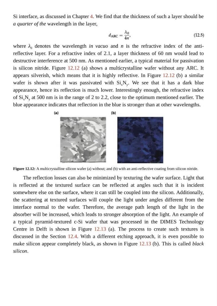
is silicon nitride. Figure 12.12 (a) shows a multicrystalline wafer without any ARC. It
appears silverish, which means that it is highly reflective. In Figure 12.12 (b) a similar
wafer is shown after it was passivated with Si x N y . We see that it has a dark blue
appearance, hence its reflection is much lower. Interestingly enough, the refractive index
of Si x N y at 500 nm is in the range of 2 to 2.2, close to the optimum mentioned earlier. The
blue appearance indicates that reflection in the blue is stronger than at other wavelengths.
Figure 12.12: A multicrystalline silicon wafer (a) without; and (b) with an anti-reflective coating from silicon nitride.
The reflection losses can also be minimized by texturing the wafer surface. Light that
is reflected at the textured surface can be reflected at angles such that it is incident
somewhere else on the surface, where it can still be coupled into the silicon. Additionally,
the scattering at textured surfaces will couple the light under angles different from the
interface normal to the wafer. Therefore, the average path length of the light in the
absorber will be increased, which leads to stronger absorption of the light. An example of
a typical pyramid-textured c-Si wafer that was processed in the DIMES Technology
Centre in Delft is shown in Figure 12.13 (a). The process to create such textures is
discussed in the Section 12.4. With a different etching approach, it is even possible to
make silicon appear completely black, as shown in Figure 12.13 (b). This is called black
silicon.
a quarter of the wavelength in the layer,
where λ 0 denotes the wavelength in vacuo and n is the refractive index of the antireflective layer. For a refractive index of 2.1, a layer thickness of 60 nm would lead to
destructive interference at 500 nm. As mentioned earlier, a typical material for passivation
is silicon nitride. Figure 12.12 (a) shows a multicrystalline wafer without any ARC. It
appears silverish, which means that it is highly reflective. In Figure 12.12 (b) a similar
wafer is shown after it was passivated with Si x N y . We see that it has a dark blue
appearance, hence its reflection is much lower. Interestingly enough, the refractive index
of Si x N y at 500 nm is in the range of 2 to 2.2, close to the optimum mentioned earlier. The
blue appearance indicates that reflection in the blue is stronger than at other wavelengths.
Figure 12.12: A multicrystalline silicon wafer (a) without; and (b) with an anti-reflective coating from silicon nitride.
The reflection losses can also be minimized by texturing the wafer surface. Light that
is reflected at the textured surface can be reflected at angles such that it is incident
somewhere else on the surface, where it can still be coupled into the silicon. Additionally,
the scattering at textured surfaces will couple the light under angles different from the
interface normal to the wafer. Therefore, the average path length of the light in the
absorber will be increased, which leads to stronger absorption of the light. An example of
a typical pyramid-textured c-Si wafer that was processed in the DIMES Technology
Centre in Delft is shown in Figure 12.13 (a). The process to create such textures is
discussed in the Section 12.4. With a different etching approach, it is even possible to
make silicon appear completely black, as shown in Figure 12.13 (b). This is called black
silicon.