

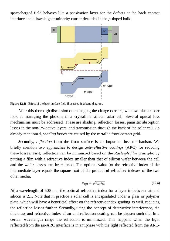
spacecharged field behaves like a passivation layer for the defects at the back contact
interface and allows higher minority carrier densities in the p-doped bulk.
Figure 12.11: Effect of the back surface field illustrated in a band diagram.
After this thorough discussion on managing the charge carriers, we now take a closer
look at managing the photons in a crystalline silicon solar cell. Several optical loss
mechanisms must be addressed. These are shading, reflection losses, parasitic absorption
losses in the non-PV-active layers, and transmission through the back of the solar cell. As
already mentioned, shading losses are caused by the metallic front contact grid.
Secondly, reflection from the front surface is an important loss mechanism. We
briefly mention two approaches to design anti-reflective coatings (ARC) for reducing
these losses. First, reflection can be minimized based on the Rayleigh film principle: by
putting a film with a refractive index smaller than that of silicon wafer between the cell
and the wafer, losses can be reduced. The optimal value for the refractive index of the
intermediate layer equals the square root of the product of refractive indexes of the two
other media,
At a wavelength of 500 nm, the optimal refractive index for a layer in-between air and
silicon is 2.1. Note that in practice a solar cell is encapsulated under a glass or polymer
plate, which will have a beneficial effect on the refractive index grading as well, reducing
the reflection losses further. Secondly, using the concept of destructive interference, the
thickness and refractive index of an anti-reflection coating can be chosen such that in a
certain wavelength range the reflection is minimized. This happens when the light
reflected from the air-ARC interface is in antiphase with the light reflected from the ARC-
interface and allows higher minority carrier densities in the p-doped bulk.
Figure 12.11: Effect of the back surface field illustrated in a band diagram.
After this thorough discussion on managing the charge carriers, we now take a closer
look at managing the photons in a crystalline silicon solar cell. Several optical loss
mechanisms must be addressed. These are shading, reflection losses, parasitic absorption
losses in the non-PV-active layers, and transmission through the back of the solar cell. As
already mentioned, shading losses are caused by the metallic front contact grid.
Secondly, reflection from the front surface is an important loss mechanism. We
briefly mention two approaches to design anti-reflective coatings (ARC) for reducing
these losses. First, reflection can be minimized based on the Rayleigh film principle: by
putting a film with a refractive index smaller than that of silicon wafer between the cell
and the wafer, losses can be reduced. The optimal value for the refractive index of the
intermediate layer equals the square root of the product of refractive indexes of the two
other media,
At a wavelength of 500 nm, the optimal refractive index for a layer in-between air and
silicon is 2.1. Note that in practice a solar cell is encapsulated under a glass or polymer
plate, which will have a beneficial effect on the refractive index grading as well, reducing
the reflection losses further. Secondly, using the concept of destructive interference, the
thickness and refractive index of an anti-reflection coating can be chosen such that in a
certain wavelength range the reflection is minimized. This happens when the light
reflected from the air-ARC interface is in antiphase with the light reflected from the ARC-