

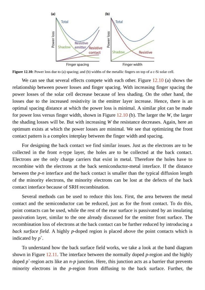
Figure 12.10: Power loss due to (a) spacing; and (b) widths of the metallic fingers on top of a c-Si solar cell.
We can see that several effects compete with each other. Figure 12.10 (a) shows the
relationship between power losses and finger spacing. With increasing finger spacing the
power losses of the solar cell decrease because of less shading. On the other hand, the
losses due to the increased resistivity in the emitter layer increase. Hence, there is an
optimal spacing distance at which the power loss is minimal. A similar plot can be made
for power loss versus finger width, shown in Figure 12.10 (b). The larger the W, the larger
the shading losses will be. But with increasing W the resistance decreases. Again, here an
optimum exists at which the power losses are minimal. We see that optimizing the front
contact pattern is a complex interplay between the finger width and spacing.
For designing the back contact we find similar issues. Just as the electrons are to be
collected in the front n-type layer, the holes are to be collected at the back contact.
Electrons are the only charge carriers that exist in metal. Therefore the holes have to
recombine with the electrons at the back semiconductor-metal interface. If the distance
between the p-n interface and the back contact is smaller than the typical diffusion length
of the minority electrons, the minority electrons can be lost at the defects of the back
contact interface because of SRH recombination.
Several methods can be used to reduce this loss. First, the area between the metal
contact and the semiconductor can be reduced, just as for the front contact. To do this,
point contacts can be used, while the rest of the rear surface is passivated by an insulating
passivation layer, similar to the one already discussed for the emitter front surface. The
recombination loss of electrons at the back contact can be further reduced by introducing a
back surface field. A highly p-doped region is placed above the point contacts which is
indicated by p
+
.
To understand how the back surface field works, we take a look at the band diagram
shown in Figure 12.11. The interface between the normally doped p-region and the highly
doped p
+
-region acts like an n-p junction. Here, this junction acts as a barrier that prevents
minority electrons in the p-region from diffusing to the back surface. Further, the
We can see that several effects compete with each other. Figure 12.10 (a) shows the
relationship between power losses and finger spacing. With increasing finger spacing the
power losses of the solar cell decrease because of less shading. On the other hand, the
losses due to the increased resistivity in the emitter layer increase. Hence, there is an
optimal spacing distance at which the power loss is minimal. A similar plot can be made
for power loss versus finger width, shown in Figure 12.10 (b). The larger the W, the larger
the shading losses will be. But with increasing W the resistance decreases. Again, here an
optimum exists at which the power losses are minimal. We see that optimizing the front
contact pattern is a complex interplay between the finger width and spacing.
For designing the back contact we find similar issues. Just as the electrons are to be
collected in the front n-type layer, the holes are to be collected at the back contact.
Electrons are the only charge carriers that exist in metal. Therefore the holes have to
recombine with the electrons at the back semiconductor-metal interface. If the distance
between the p-n interface and the back contact is smaller than the typical diffusion length
of the minority electrons, the minority electrons can be lost at the defects of the back
contact interface because of SRH recombination.
Several methods can be used to reduce this loss. First, the area between the metal
contact and the semiconductor can be reduced, just as for the front contact. To do this,
point contacts can be used, while the rest of the rear surface is passivated by an insulating
passivation layer, similar to the one already discussed for the emitter front surface. The
recombination loss of electrons at the back contact can be further reduced by introducing a
back surface field. A highly p-doped region is placed above the point contacts which is
indicated by p
+
.
To understand how the back surface field works, we take a look at the band diagram
shown in Figure 12.11. The interface between the normally doped p-region and the highly
doped p
+
-region acts like an n-p junction. Here, this junction acts as a barrier that prevents
minority electrons in the p-region from diffusing to the back surface. Further, the