

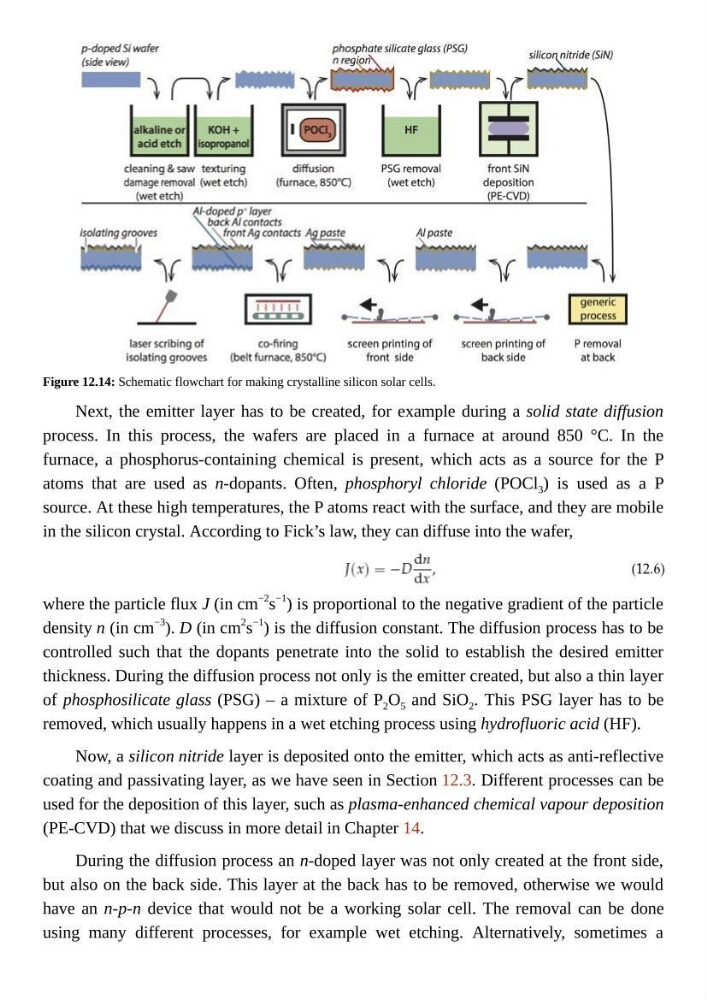
Figure 12.14: Schematic flowchart for making crystalline silicon solar cells.
Next, the emitter layer has to be created, for example during a solid state diffusion
process. In this process, the wafers are placed in a furnace at around 850 °C. In the
furnace, a phosphorus-containing chemical is present, which acts as a source for the P
atoms that are used as n-dopants. Often, phosphoryl chloride (POCl 3 ) is used as a P
source. At these high temperatures, the P atoms react with the surface, and they are mobile
in the silicon crystal. According to Fick’s law, they can diffuse into the wafer,
where the particle flux J (in cm
−2 s
−1
) is proportional to the negative gradient of the particle
density n (in cm
−3
). D (in cm
2
s
−1 ) is the diffusion constant. The diffusion process has to be
controlled such that the dopants penetrate into the solid to establish the desired emitter
thickness. During the diffusion process not only is the emitter created, but also a thin layer
of phosphosilicate glass (PSG) – a mixture of P 2 O 5 and SiO 2 . This PSG layer has to be
removed, which usually happens in a wet etching process using hydrofluoric acid (HF).
Now, a silicon nitride layer is deposited onto the emitter, which acts as anti-reflective
coating and passivating layer, as we have seen in Section 12.3. Different processes can be
used for the deposition of this layer, such as plasma-enhanced chemical vapour deposition
(PE-CVD) that we discuss in more detail in Chapter 14.
During the diffusion process an n-doped layer was not only created at the front side,
but also on the back side. This layer at the back has to be removed, otherwise we would
have an n-p-n device that would not be a working solar cell. The removal can be done
using many different processes, for example wet etching. Alternatively, sometimes a
Next, the emitter layer has to be created, for example during a solid state diffusion
process. In this process, the wafers are placed in a furnace at around 850 °C. In the
furnace, a phosphorus-containing chemical is present, which acts as a source for the P
atoms that are used as n-dopants. Often, phosphoryl chloride (POCl 3 ) is used as a P
source. At these high temperatures, the P atoms react with the surface, and they are mobile
in the silicon crystal. According to Fick’s law, they can diffuse into the wafer,
where the particle flux J (in cm
−2 s
−1
) is proportional to the negative gradient of the particle
density n (in cm
−3
). D (in cm
2
s
−1 ) is the diffusion constant. The diffusion process has to be
controlled such that the dopants penetrate into the solid to establish the desired emitter
thickness. During the diffusion process not only is the emitter created, but also a thin layer
of phosphosilicate glass (PSG) – a mixture of P 2 O 5 and SiO 2 . This PSG layer has to be
removed, which usually happens in a wet etching process using hydrofluoric acid (HF).
Now, a silicon nitride layer is deposited onto the emitter, which acts as anti-reflective
coating and passivating layer, as we have seen in Section 12.3. Different processes can be
used for the deposition of this layer, such as plasma-enhanced chemical vapour deposition
(PE-CVD) that we discuss in more detail in Chapter 14.
During the diffusion process an n-doped layer was not only created at the front side,
but also on the back side. This layer at the back has to be removed, otherwise we would
have an n-p-n device that would not be a working solar cell. The removal can be done
using many different processes, for example wet etching. Alternatively, sometimes a