

differentiate between two major types of silicon wafers: monocrystalline silicon and
multicrystalline silicon, which is also called polycrystalline silicon.
Monocrystalline silicon, also known as single-crystalline silicon, is a crystalline solid
in which the crystal lattice is continuous and unbroken without any grain boundaries over
the entire bulk, up to the edges. In contrast, polycrystalline silicon, often simply
abbreviated as polysilicon, is a material that consists of many small crystalline grains, with
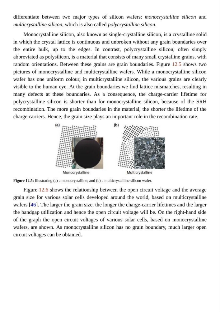
random orientations. Between these grains are grain boundaries. Figure 12.5 shows two
pictures of monocrystalline and multicrystalline wafers. While a monocrystalline silicon
wafer has one uniform colour, in multicrystalline silicon, the various grains are clearly
visible to the human eye. At the grain boundaries we find lattice mismatches, resulting in
many defects at these boundaries. As a consequence, the charge-carrier lifetime for
polycrystalline silicon is shorter than for monocrystalline silicon, because of the SRH
recombination. The more grain boundaries in the material, the shorter the lifetime of the
charge carriers. Hence, the grain size plays an important role in the recombination rate.
Figure 12.5: Illustrating (a) a monocrystalline; and (b) a multicrystalline silicon wafer.
Figure 12.6 shows the relationship between the open circuit voltage and the average
grain size for various solar cells developed around the world, based on multicrystalline
wafers [46]. The larger the grain size, the longer the charge-carrier lifetimes and the larger
the bandgap utilization and hence the open circuit voltage will be. On the right-hand side
of the graph the open circuit voltages of various solar cells, based on monocrystalline
wafers, are shown. As monocrystalline silicon has no grain boundary, much larger open
circuit voltages can be obtained.
multicrystalline silicon, which is also called polycrystalline silicon.
Monocrystalline silicon, also known as single-crystalline silicon, is a crystalline solid
in which the crystal lattice is continuous and unbroken without any grain boundaries over
the entire bulk, up to the edges. In contrast, polycrystalline silicon, often simply
abbreviated as polysilicon, is a material that consists of many small crystalline grains, with
random orientations. Between these grains are grain boundaries. Figure 12.5 shows two
pictures of monocrystalline and multicrystalline wafers. While a monocrystalline silicon
wafer has one uniform colour, in multicrystalline silicon, the various grains are clearly
visible to the human eye. At the grain boundaries we find lattice mismatches, resulting in
many defects at these boundaries. As a consequence, the charge-carrier lifetime for
polycrystalline silicon is shorter than for monocrystalline silicon, because of the SRH
recombination. The more grain boundaries in the material, the shorter the lifetime of the
charge carriers. Hence, the grain size plays an important role in the recombination rate.
Figure 12.5: Illustrating (a) a monocrystalline; and (b) a multicrystalline silicon wafer.
Figure 12.6 shows the relationship between the open circuit voltage and the average
grain size for various solar cells developed around the world, based on multicrystalline
wafers [46]. The larger the grain size, the longer the charge-carrier lifetimes and the larger
the bandgap utilization and hence the open circuit voltage will be. On the right-hand side
of the graph the open circuit voltages of various solar cells, based on monocrystalline
wafers, are shown. As monocrystalline silicon has no grain boundary, much larger open
circuit voltages can be obtained.