

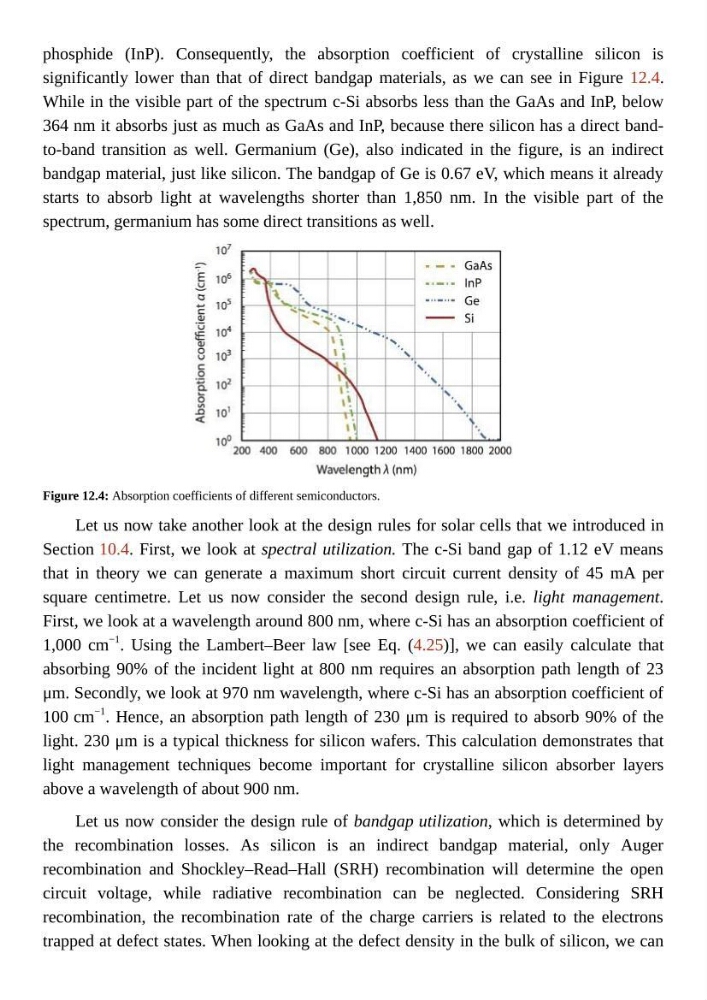
phosphide (InP). Consequently, the absorption coefficient of crystalline silicon is
significantly lower than that of direct bandgap materials, as we can see in Figure 12.4.
While in the visible part of the spectrum c-Si absorbs less than the GaAs and InP, below
364 nm it absorbs just as much as GaAs and InP, because there silicon has a direct bandto-band transition as well. Germanium (Ge), also indicated in the figure, is an indirect
bandgap material, just like silicon. The bandgap of Ge is 0.67 eV, which means it already
starts to absorb light at wavelengths shorter than 1,850 nm. In the visible part of the
spectrum, germanium has some direct transitions as well.
Figure 12.4: Absorption coefficients of different semiconductors.
Let us now take another look at the design rules for solar cells that we introduced in
Section 10.4. First, we look at spectral utilization. The c-Si band gap of 1.12 eV means
that in theory we can generate a maximum short circuit current density of 45 mA per
square centimetre. Let us now consider the second design rule, i.e. light management.
First, we look at a wavelength around 800 nm, where c-Si has an absorption coefficient of
1,000 cm
−1 . Using the Lambert–Beer law [see Eq. (4.25)], we can easily calculate that
absorbing 90% of the incident light at 800 nm requires an absorption path length of 23
μm. Secondly, we look at 970 nm wavelength, where c-Si has an absorption coefficient of
100 cm
−1 . Hence, an absorption path length of 230 μm is required to absorb 90% of the
light. 230 μm is a typical thickness for silicon wafers. This calculation demonstrates that
light management techniques become important for crystalline silicon absorber layers
above a wavelength of about 900 nm.
Let us now consider the design rule of bandgap utilization, which is determined by
the recombination losses. As silicon is an indirect bandgap material, only Auger
recombination and Shockley–Read–Hall (SRH) recombination will determine the open
circuit voltage, while radiative recombination can be neglected. Considering SRH
recombination, the recombination rate of the charge carriers is related to the electrons
trapped at defect states. When looking at the defect density in the bulk of silicon, we can
significantly lower than that of direct bandgap materials, as we can see in Figure 12.4.
While in the visible part of the spectrum c-Si absorbs less than the GaAs and InP, below
364 nm it absorbs just as much as GaAs and InP, because there silicon has a direct bandto-band transition as well. Germanium (Ge), also indicated in the figure, is an indirect
bandgap material, just like silicon. The bandgap of Ge is 0.67 eV, which means it already
starts to absorb light at wavelengths shorter than 1,850 nm. In the visible part of the
spectrum, germanium has some direct transitions as well.
Figure 12.4: Absorption coefficients of different semiconductors.
Let us now take another look at the design rules for solar cells that we introduced in
Section 10.4. First, we look at spectral utilization. The c-Si band gap of 1.12 eV means
that in theory we can generate a maximum short circuit current density of 45 mA per
square centimetre. Let us now consider the second design rule, i.e. light management.
First, we look at a wavelength around 800 nm, where c-Si has an absorption coefficient of
1,000 cm
−1 . Using the Lambert–Beer law [see Eq. (4.25)], we can easily calculate that
absorbing 90% of the incident light at 800 nm requires an absorption path length of 23
μm. Secondly, we look at 970 nm wavelength, where c-Si has an absorption coefficient of
100 cm
−1 . Hence, an absorption path length of 230 μm is required to absorb 90% of the
light. 230 μm is a typical thickness for silicon wafers. This calculation demonstrates that
light management techniques become important for crystalline silicon absorber layers
above a wavelength of about 900 nm.
Let us now consider the design rule of bandgap utilization, which is determined by
the recombination losses. As silicon is an indirect bandgap material, only Auger
recombination and Shockley–Read–Hall (SRH) recombination will determine the open
circuit voltage, while radiative recombination can be neglected. Considering SRH
recombination, the recombination rate of the charge carriers is related to the electrons
trapped at defect states. When looking at the defect density in the bulk of silicon, we can