

Figure 12.2: The (a) 100; and (b) 111 surfaces of a silicon crystal.
To understand the importance of these directions, we look at the electronic band
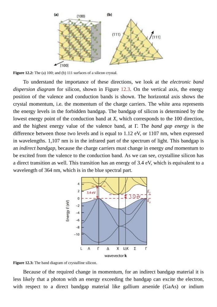
dispersion diagram for silicon, shown in Figure 12.3. On the vertical axis, the energy
position of the valence and conduction bands is shown. The horizontal axis shows the
crystal momentum, i.e. the momentum of the charge carriers. The white area represents
the energy levels in the forbidden bandgap. The bandgap of silicon is determined by the
lowest energy point of the conduction band at X, which corresponds to the 100 direction,
and the highest energy value of the valence band, at Γ. The band gap energy is the
difference between those two levels and is equal to 1.12 eV, or 1107 nm, when expressed
in wavelengths. 1,107 nm is in the infrared part of the spectrum of light. This bandgap is
an indirect bandgap, because the charge carriers must change in energy and momentum to
be excited from the valence to the conduction band. As we can see, crystalline silicon has
a direct transition as well. This transition has an energy of 3.4 eV, which is equivalent to a
wavelength of 364 nm, which is in the blue spectral part.
Figure 12.3: The band diagram of crystalline silicon.
Because of the required change in momentum, for an indirect bandgap material it is
less likely that a photon with an energy exceeding the bandgap can excite the electron,
with respect to a direct bandgap material like gallium arsenide (GaAs) or indium
To understand the importance of these directions, we look at the electronic band
dispersion diagram for silicon, shown in Figure 12.3. On the vertical axis, the energy
position of the valence and conduction bands is shown. The horizontal axis shows the
crystal momentum, i.e. the momentum of the charge carriers. The white area represents
the energy levels in the forbidden bandgap. The bandgap of silicon is determined by the
lowest energy point of the conduction band at X, which corresponds to the 100 direction,
and the highest energy value of the valence band, at Γ. The band gap energy is the
difference between those two levels and is equal to 1.12 eV, or 1107 nm, when expressed
in wavelengths. 1,107 nm is in the infrared part of the spectrum of light. This bandgap is
an indirect bandgap, because the charge carriers must change in energy and momentum to
be excited from the valence to the conduction band. As we can see, crystalline silicon has
a direct transition as well. This transition has an energy of 3.4 eV, which is equivalent to a
wavelength of 364 nm, which is in the blue spectral part.
Figure 12.3: The band diagram of crystalline silicon.
Because of the required change in momentum, for an indirect bandgap material it is
less likely that a photon with an energy exceeding the bandgap can excite the electron,
with respect to a direct bandgap material like gallium arsenide (GaAs) or indium