

12.1
12
Crystalline silicon solar cells
As we already discussed in Chapter 6, most semiconductor materials have a crystalline
lattice structure. As a starting point for our discussion on crystalline silicon PV
technology, we will take a closer look at some properties of the crystal lattice.
Crystalline silicon
In such a lattice, the atoms are arranged in a certain pattern that repeats itself. The lattice
thus has long-range order and symmetry. However, the pattern is not the same in every
direction. In other words, if we make large cuts through the lattice, the various planes
would not look the same.
Crystalline silicon has a density of 2.3290 g/cm
3 and a diamond cubic crystal
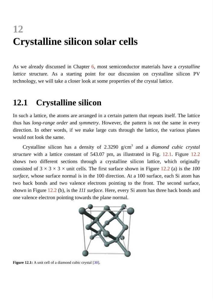
structure with a lattice constant of 543.07 pm, as illustrated in Fig. 12.1. Figure 12.2
shows two different sections through a crystalline silicon lattice, which originally
consisted of 3 × 3 × 3 × unit cells. The first surface shown in Figure 12.2 (a) is the 100
surface, whose surface normal is in the 100 direction. At a 100 surface, each Si atom has
two back bonds and two valence electrons pointing to the front. The second surface,
shown in Figure 12.2 (b), is the 111 surface. Here, every Si atom has three back bonds and
one valence electron pointing towards the plane normal.
Figure 12.1: A unit cell of a diamond cubic crystal [30].
12
Crystalline silicon solar cells
As we already discussed in Chapter 6, most semiconductor materials have a crystalline
lattice structure. As a starting point for our discussion on crystalline silicon PV
technology, we will take a closer look at some properties of the crystal lattice.
Crystalline silicon
In such a lattice, the atoms are arranged in a certain pattern that repeats itself. The lattice
thus has long-range order and symmetry. However, the pattern is not the same in every
direction. In other words, if we make large cuts through the lattice, the various planes
would not look the same.
Crystalline silicon has a density of 2.3290 g/cm
3 and a diamond cubic crystal
structure with a lattice constant of 543.07 pm, as illustrated in Fig. 12.1. Figure 12.2
shows two different sections through a crystalline silicon lattice, which originally
consisted of 3 × 3 × 3 × unit cells. The first surface shown in Figure 12.2 (a) is the 100
surface, whose surface normal is in the 100 direction. At a 100 surface, each Si atom has
two back bonds and two valence electrons pointing to the front. The second surface,
shown in Figure 12.2 (b), is the 111 surface. Here, every Si atom has three back bonds and
one valence electron pointing towards the plane normal.
Figure 12.1: A unit cell of a diamond cubic crystal [30].