

8.5
(a)
(b)
(c)
(d)
8.6
(a)
(b)
(c)
(d)
(e)
8.7
(a)
(b)
(c)
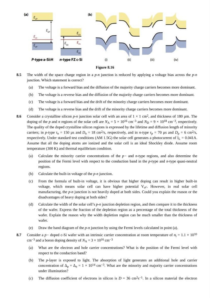
Figure 8.16
The width of the space charge region in a p-n junction is reduced by applying a voltage bias across the p-n
junction. Which statement is correct?
The voltage is a forward bias and the diffusion of the majority charge carriers becomes more dominant.
The voltage is a reverse bias and the diffusion of the majority charge carriers becomes more dominant.
The voltage is a forward bias and the drift of the minority charge carriers becomes more dominant.
The voltage is a reverse bias and the drift of the minority charge carriers becomes more dominant.
Consider a crystalline silicon p-n junction solar cell with an area of 1 × 1 cm 2 , and thickness of 180 µm. The
doping of the p and n regions of the solar cell are N A = 5 × 10 16 cm −3 and N D = 9 × 10 18 cm −3 , respectively.
The quality of the doped crystalline silicon regions is expressed by the lifetime and diffusion length of minority
carriers; in p-type τ n = 150 µs and D n = 18 cm 2 /s, respectively, and in n-type τ p = 70 µs and D p = 6 cm 2 /s,
respectively. Under standard test conditions (AM 1.5G) the solar cell generates a photocurrent of I L = 0.041A.
Assume that all the doping atoms are ionized and the solar cell is an ideal Shockley diode. Assume room
temperature (300 K) and thermal equilibrium condition.
Calculate the minority carrier concentrations of the p− and n-type regions, and also determine the
position of the Fermi level with respect to the conduction band in the p-type and n-type quasi-neutral
regions.
Calculate the built-in voltage of the p-n junction.
From the formula of built-in voltage, it is obvious that higher doping can result in higher built-in
voltage, which means solar cell can have higher potential V o c. However, in real solar cell
manufacturing, the p-n junction is not heavily doped at both sides. Could you explain the reason or the
disadvantages of heavy doping at both sides?
Calculate the width of the solar cell’s p-n junction depletion region, and then compare it to the thickness
of the wafer. Express the fraction of the depletion region as a percentage of the total thickness of the
wafer. Explain the reason why the width depletion region can be much smaller than the thickness of
wafer.
Draw the band diagram of the p-n junction by using the Fermi levels calculated in point (a).
Consider a p− doped c-Si wafer with an intrinsic carrier concentration at room temperature of n i = 1.1 × 10 10
cm −3 and a boron doping density of N A = 3 × 10 16 cm −3
What are the electron and hole carrier concentrations? What is the position of the Fermi level with
respect to the conduction band?
The p-layer is exposed to light. The absorption of light generates an additional hole and carrier
concentration of Δ p = Δ n = 1 × 10 14 cm −3 . What are the minority and majority carrier concentrations
under illumination?
The diffusion coefficient of electrons in silicon is D = 36 cm 2 s −1 . In a silicon material the electron
(a)
(b)
(c)
(d)
8.6
(a)
(b)
(c)
(d)
(e)
8.7
(a)
(b)
(c)
Figure 8.16
The width of the space charge region in a p-n junction is reduced by applying a voltage bias across the p-n
junction. Which statement is correct?
The voltage is a forward bias and the diffusion of the majority charge carriers becomes more dominant.
The voltage is a reverse bias and the diffusion of the majority charge carriers becomes more dominant.
The voltage is a forward bias and the drift of the minority charge carriers becomes more dominant.
The voltage is a reverse bias and the drift of the minority charge carriers becomes more dominant.
Consider a crystalline silicon p-n junction solar cell with an area of 1 × 1 cm 2 , and thickness of 180 µm. The
doping of the p and n regions of the solar cell are N A = 5 × 10 16 cm −3 and N D = 9 × 10 18 cm −3 , respectively.
The quality of the doped crystalline silicon regions is expressed by the lifetime and diffusion length of minority
carriers; in p-type τ n = 150 µs and D n = 18 cm 2 /s, respectively, and in n-type τ p = 70 µs and D p = 6 cm 2 /s,
respectively. Under standard test conditions (AM 1.5G) the solar cell generates a photocurrent of I L = 0.041A.
Assume that all the doping atoms are ionized and the solar cell is an ideal Shockley diode. Assume room
temperature (300 K) and thermal equilibrium condition.
Calculate the minority carrier concentrations of the p− and n-type regions, and also determine the
position of the Fermi level with respect to the conduction band in the p-type and n-type quasi-neutral
regions.
Calculate the built-in voltage of the p-n junction.
From the formula of built-in voltage, it is obvious that higher doping can result in higher built-in
voltage, which means solar cell can have higher potential V o c. However, in real solar cell
manufacturing, the p-n junction is not heavily doped at both sides. Could you explain the reason or the
disadvantages of heavy doping at both sides?
Calculate the width of the solar cell’s p-n junction depletion region, and then compare it to the thickness
of the wafer. Express the fraction of the depletion region as a percentage of the total thickness of the
wafer. Explain the reason why the width depletion region can be much smaller than the thickness of
wafer.
Draw the band diagram of the p-n junction by using the Fermi levels calculated in point (a).
Consider a p− doped c-Si wafer with an intrinsic carrier concentration at room temperature of n i = 1.1 × 10 10
cm −3 and a boron doping density of N A = 3 × 10 16 cm −3
What are the electron and hole carrier concentrations? What is the position of the Fermi level with
respect to the conduction band?
The p-layer is exposed to light. The absorption of light generates an additional hole and carrier
concentration of Δ p = Δ n = 1 × 10 14 cm −3 . What are the minority and majority carrier concentrations
under illumination?
The diffusion coefficient of electrons in silicon is D = 36 cm 2 s −1 . In a silicon material the electron