

8.4
8.1
(a)
(b)
(c)
8.2
8.3
(a)
(b)
(c)
(d)
8.4
Exercises
The p-type region of a silicon p-n junction is doped with 10 16 boron atoms per cubic centimetre, and the n-type
region is doped with 10 18 phosphorus atoms per cubic centimetre. Assume a step p-n junction and that all
doping atoms are ionized. The intrinsic carrier concentration in silicon at 300 K is 1.5 × 10 10 cm −3 .
What are the electron and hole concentrations in the p- and n-type regions at thermal equilibrium?
Calculate the built-in voltage V bi at 300 K.
Calculate the width of the depletion region at 300 K (the relative permittivity of Si is ∈ r = 11.7).
A crystalline silicon solar cell generates a photocurrent density of J ph = 35 mA/cm 2 at T = 300 K. The
saturation current density is J 0 = 1.95 × 10 −10 mA/cm 2 . Assuming that the solar cell behaves as an ideal p-n
junction, calculate the open circuit voltage V oc .
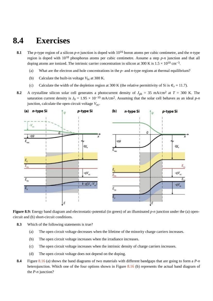
Figure 8.9: Energy band diagram and electrostatic-potential (in green) of an illuminated p-n junction under the (a) opencircuit and (b) short-circuit conditions.
Which of the following statements is true?
The open circuit voltage decreases when the lifetime of the minority charge carriers increases.
The open circuit voltage increases when the irradiance increases.
The open circuit voltage increases when the intrinsic density of charge carriers increases.
The open circuit voltage does not depend on the doping.
Figure 8.16 (a) shows the band diagrams of two materials with different bandgaps that are going to form a P-n
heterojunction. Which one of the four options shown in Figure 8.16 (b) represents the actual band diagram of
the P-n junction?
8.1
(a)
(b)
(c)
8.2
8.3
(a)
(b)
(c)
(d)
8.4
Exercises
The p-type region of a silicon p-n junction is doped with 10 16 boron atoms per cubic centimetre, and the n-type
region is doped with 10 18 phosphorus atoms per cubic centimetre. Assume a step p-n junction and that all
doping atoms are ionized. The intrinsic carrier concentration in silicon at 300 K is 1.5 × 10 10 cm −3 .
What are the electron and hole concentrations in the p- and n-type regions at thermal equilibrium?
Calculate the built-in voltage V bi at 300 K.
Calculate the width of the depletion region at 300 K (the relative permittivity of Si is ∈ r = 11.7).
A crystalline silicon solar cell generates a photocurrent density of J ph = 35 mA/cm 2 at T = 300 K. The
saturation current density is J 0 = 1.95 × 10 −10 mA/cm 2 . Assuming that the solar cell behaves as an ideal p-n
junction, calculate the open circuit voltage V oc .
Figure 8.9: Energy band diagram and electrostatic-potential (in green) of an illuminated p-n junction under the (a) opencircuit and (b) short-circuit conditions.
Which of the following statements is true?
The open circuit voltage decreases when the lifetime of the minority charge carriers increases.
The open circuit voltage increases when the irradiance increases.
The open circuit voltage increases when the intrinsic density of charge carriers increases.
The open circuit voltage does not depend on the doping.
Figure 8.16 (a) shows the band diagrams of two materials with different bandgaps that are going to form a P-n
heterojunction. Which one of the four options shown in Figure 8.16 (b) represents the actual band diagram of
the P-n junction?