

Figure 8.12 (b). For an n-type semiconductor, the height of this barrier is given by
In the case of a p-type semiconductor we find
As a result of Eqs. (8.43), the sum of the barrier heights of n- and p-type substrates of a
semiconductor is equal to its bandgap,
Note that this result is independent of the metal. An electron that wants to travel from the
conduction band of the semiconductor to the metal experiences a built-in voltage,
where φ n is the distance between the lower edge of the conduction band and the Fermi
level of the n-type semiconductor.
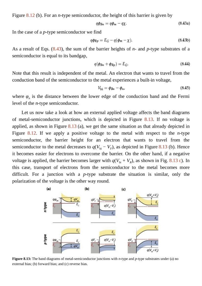
Let us now take a look at how an external applied voltage affects the band diagrams
of metal-semiconductor junctions, which is depicted in Figure 8.13. If no voltage is
applied, as shown in Figure 8.13 (a), we get the same situation as that already depicted in
Figure 8.12. If we apply a positive voltage to the metal with respect to the n-type
semiconductor, the barrier height for an electron that wants to travel from the
semiconductor to the metal decreases to q(V bi − V F ), as depicted in Figure 8.13 (b). Hence
it becomes easier for electrons to overcome the barrier. On the other hand, if a negative
voltage is applied, the barrier becomes larger with q(V bi + V R ), as shown in Fig. 8.13 c). In
this case, transport of electrons from the semiconductor to the metal becomes more
difficult. For a junction with a p-type substrate the situation is similar, only the
polarization of the voltage is the other way round.
Figure 8.13: The band diagrams of metal-semiconductor junctions with n-type and p-type substrates under (a) no
external bias; (b) forward bias; and (c) reverse bias.
In the case of a p-type semiconductor we find
As a result of Eqs. (8.43), the sum of the barrier heights of n- and p-type substrates of a
semiconductor is equal to its bandgap,
Note that this result is independent of the metal. An electron that wants to travel from the
conduction band of the semiconductor to the metal experiences a built-in voltage,
where φ n is the distance between the lower edge of the conduction band and the Fermi
level of the n-type semiconductor.
Let us now take a look at how an external applied voltage affects the band diagrams
of metal-semiconductor junctions, which is depicted in Figure 8.13. If no voltage is
applied, as shown in Figure 8.13 (a), we get the same situation as that already depicted in
Figure 8.12. If we apply a positive voltage to the metal with respect to the n-type
semiconductor, the barrier height for an electron that wants to travel from the
semiconductor to the metal decreases to q(V bi − V F ), as depicted in Figure 8.13 (b). Hence
it becomes easier for electrons to overcome the barrier. On the other hand, if a negative
voltage is applied, the barrier becomes larger with q(V bi + V R ), as shown in Fig. 8.13 c). In
this case, transport of electrons from the semiconductor to the metal becomes more
difficult. For a junction with a p-type substrate the situation is similar, only the
polarization of the voltage is the other way round.
Figure 8.13: The band diagrams of metal-semiconductor junctions with n-type and p-type substrates under (a) no
external bias; (b) forward bias; and (c) reverse bias.