

8.3.1
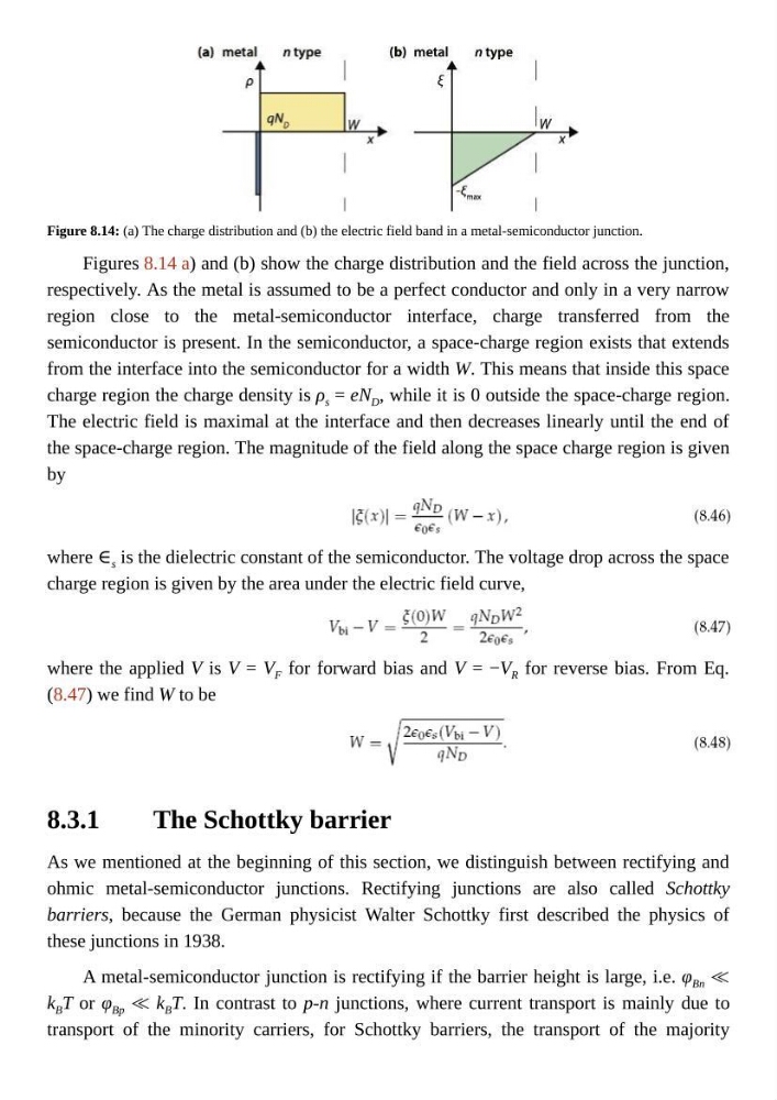
Figure 8.14: (a) The charge distribution and (b) the electric field band in a metal-semiconductor junction.
Figures 8.14 a) and (b) show the charge distribution and the field across the junction,
respectively. As the metal is assumed to be a perfect conductor and only in a very narrow
region close to the metal-semiconductor interface, charge transferred from the
semiconductor is present. In the semiconductor, a space-charge region exists that extends
from the interface into the semiconductor for a width W. This means that inside this space
charge region the charge density is ρ s = eN D , while it is 0 outside the space-charge region.
The electric field is maximal at the interface and then decreases linearly until the end of
the space-charge region. The magnitude of the field along the space charge region is given
by
where ∈ s is the dielectric constant of the semiconductor. The voltage drop across the space
charge region is given by the area under the electric field curve,
where the applied V is V = V F for forward bias and V = −V R for reverse bias. From Eq.
(8.47) we find W to be
The Schottky barrier
As we mentioned at the beginning of this section, we distinguish between rectifying and
ohmic metal-semiconductor junctions. Rectifying junctions are also called Schottky
barriers, because the German physicist Walter Schottky first described the physics of
these junctions in 1938.
A metal-semiconductor junction is rectifying if the barrier height is large, i.e. φ Bn ≪
k B T or φ Bp ≪ k B T. In contrast to p-n junctions, where current transport is mainly due to
transport of the minority carriers, for Schottky barriers, the transport of the majority
Figure 8.14: (a) The charge distribution and (b) the electric field band in a metal-semiconductor junction.
Figures 8.14 a) and (b) show the charge distribution and the field across the junction,
respectively. As the metal is assumed to be a perfect conductor and only in a very narrow
region close to the metal-semiconductor interface, charge transferred from the
semiconductor is present. In the semiconductor, a space-charge region exists that extends
from the interface into the semiconductor for a width W. This means that inside this space
charge region the charge density is ρ s = eN D , while it is 0 outside the space-charge region.
The electric field is maximal at the interface and then decreases linearly until the end of
the space-charge region. The magnitude of the field along the space charge region is given
by
where ∈ s is the dielectric constant of the semiconductor. The voltage drop across the space
charge region is given by the area under the electric field curve,
where the applied V is V = V F for forward bias and V = −V R for reverse bias. From Eq.
(8.47) we find W to be
The Schottky barrier
As we mentioned at the beginning of this section, we distinguish between rectifying and
ohmic metal-semiconductor junctions. Rectifying junctions are also called Schottky
barriers, because the German physicist Walter Schottky first described the physics of
these junctions in 1938.
A metal-semiconductor junction is rectifying if the barrier height is large, i.e. φ Bn ≪
k B T or φ Bp ≪ k B T. In contrast to p-n junctions, where current transport is mainly due to
transport of the minority carriers, for Schottky barriers, the transport of the majority