

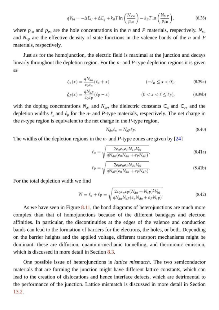
where p n0 and p P0 are the hole concentrations in the n and P materials, respectively. N Vn
and N VP are the effective density of state functions in the valence bands of the n and P
materials, respectively.
Just as for the homojunction, the electric field is maximal at the junction and decays
linearly throughout the depletion region. For the n- and P-type depletion regions it is given
as
with the doping concentrations N dn and N aP , the dielectric constants ∈ n and ∈ P , and the
depletion widths ℓ n and ℓ P for the n- and P-type materials, respectively. The net charge in
the n-type region is equivalent to the net charge in the P-type region,
The widths of the depletion regions in the n- and P-type zones are given by [24]
For the total depletion width we find
As we have seen in Figure 8.11, the band diagrams of heterojunctions are much more
complex than that of homojunctions because of the different bandgaps and electron
affinities. In particular, the discontinuities at the edges of the valence and conduction
bands can lead to the formation of barriers for the electrons, the holes, or both. Depending
on the barrier heights and the applied voltage, different transport mechanisms might be
dominant: these are diffusion, quantum-mechanic tunnelling, and thermionic emission,
which is discussed in more detail in Section 8.3.
One possible issue of heterojunctions is lattice mismatch. The two semiconductor
materials that are forming the junction might have different lattice constants, which can
lead to the creation of dislocations and hence interface defects, which are detrimental to
the performance of the junction. Lattice mismatch is discussed in more detail in Section
13.2.
and N VP are the effective density of state functions in the valence bands of the n and P
materials, respectively.
Just as for the homojunction, the electric field is maximal at the junction and decays
linearly throughout the depletion region. For the n- and P-type depletion regions it is given
as
with the doping concentrations N dn and N aP , the dielectric constants ∈ n and ∈ P , and the
depletion widths ℓ n and ℓ P for the n- and P-type materials, respectively. The net charge in
the n-type region is equivalent to the net charge in the P-type region,
The widths of the depletion regions in the n- and P-type zones are given by [24]
For the total depletion width we find
As we have seen in Figure 8.11, the band diagrams of heterojunctions are much more
complex than that of homojunctions because of the different bandgaps and electron
affinities. In particular, the discontinuities at the edges of the valence and conduction
bands can lead to the formation of barriers for the electrons, the holes, or both. Depending
on the barrier heights and the applied voltage, different transport mechanisms might be
dominant: these are diffusion, quantum-mechanic tunnelling, and thermionic emission,
which is discussed in more detail in Section 8.3.
One possible issue of heterojunctions is lattice mismatch. The two semiconductor
materials that are forming the junction might have different lattice constants, which can
lead to the creation of dislocations and hence interface defects, which are detrimental to
the performance of the junction. Lattice mismatch is discussed in more detail in Section
13.2.