

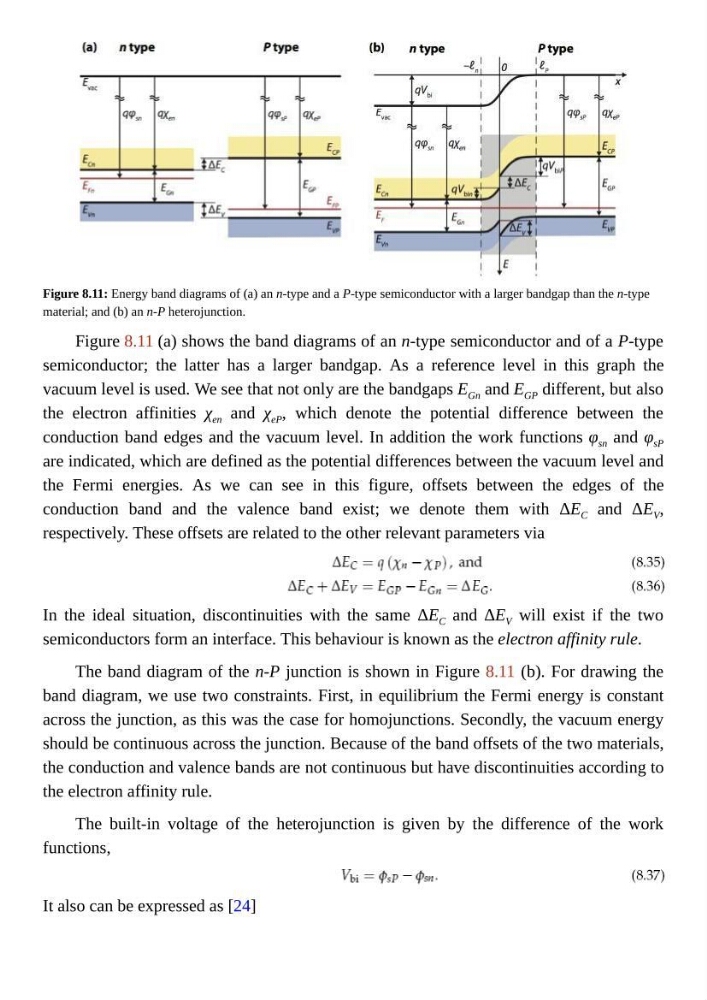
Figure 8.11: Energy band diagrams of (a) an n-type and a P-type semiconductor with a larger bandgap than the n-type
material; and (b) an n-P heterojunction.
Figure 8.11 (a) shows the band diagrams of an n-type semiconductor and of a P-type
semiconductor; the latter has a larger bandgap. As a reference level in this graph the
vacuum level is used. We see that not only are the bandgaps E Gn and E GP different, but also
the electron affinities χ en and χ eP , which denote the potential difference between the
conduction band edges and the vacuum level. In addition the work functions φ sn and φ sP
are indicated, which are defined as the potential differences between the vacuum level and
the Fermi energies. As we can see in this figure, offsets between the edges of the
conduction band and the valence band exist; we denote them with ΔE C and ΔE V ,
respectively. These offsets are related to the other relevant parameters via
In the ideal situation, discontinuities with the same ΔE C and ΔE V will exist if the two
semiconductors form an interface. This behaviour is known as the electron affinity rule.
The band diagram of the n-P junction is shown in Figure 8.11 (b). For drawing the
band diagram, we use two constraints. First, in equilibrium the Fermi energy is constant
across the junction, as this was the case for homojunctions. Secondly, the vacuum energy
should be continuous across the junction. Because of the band offsets of the two materials,
the conduction and valence bands are not continuous but have discontinuities according to
the electron affinity rule.
The built-in voltage of the heterojunction is given by the difference of the work
functions,
It also can be expressed as [24]
material; and (b) an n-P heterojunction.
Figure 8.11 (a) shows the band diagrams of an n-type semiconductor and of a P-type
semiconductor; the latter has a larger bandgap. As a reference level in this graph the
vacuum level is used. We see that not only are the bandgaps E Gn and E GP different, but also
the electron affinities χ en and χ eP , which denote the potential difference between the
conduction band edges and the vacuum level. In addition the work functions φ sn and φ sP
are indicated, which are defined as the potential differences between the vacuum level and
the Fermi energies. As we can see in this figure, offsets between the edges of the
conduction band and the valence band exist; we denote them with ΔE C and ΔE V ,
respectively. These offsets are related to the other relevant parameters via
In the ideal situation, discontinuities with the same ΔE C and ΔE V will exist if the two
semiconductors form an interface. This behaviour is known as the electron affinity rule.
The band diagram of the n-P junction is shown in Figure 8.11 (b). For drawing the
band diagram, we use two constraints. First, in equilibrium the Fermi energy is constant
across the junction, as this was the case for homojunctions. Secondly, the vacuum energy
should be continuous across the junction. Because of the band offsets of the two materials,
the conduction and valence bands are not continuous but have discontinuities according to
the electron affinity rule.
The built-in voltage of the heterojunction is given by the difference of the work
functions,
It also can be expressed as [24]