

77
Process-Induced Stress Engineering in CMOS Technology
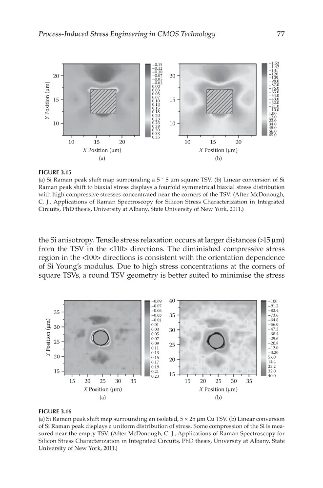
the Si anisotropy. Tensile stress relaxation occurs at larger distances (>15 μm)
from the TSV in the <110> directions. The diminished compressive stress
region in the <100> directions is consistent with the orientation dependence
of Si Young’s modulus. Due to high stress concentrations at the corners of
square TSVs, a round TSV geometry is better suited to minimise the stress
20
15
10
20
–0.15
–0.12
–0.10
–0.07
–0.05
–0.02
0.00
0.03
0.05
0.07
0.10
0.13
0.15
0.18
0.20
0.23
0.25
0.28
0.30
0.33
0.35
–1.53
–1.42
–131
–120
–109
–98.0
–87.0
–76.0
–65.0
–54.0
–43.0
–32.0
–21.0
–10.0
1.00
12.0
23.0
34.0
45.0
56.0
65.0
15
10
10
15
X Position (µm)
Y Position (µm)
20
10
15
X Position (µm)
(a)
(b)
20
FIGURE 3.15
(a) Si Raman peak shift map surrounding a 5 ´ 5 μm square TSV. (b) Linear conversion of Si
Raman peak shift to biaxial stress displays a fourfold symmetrical biaxial stress distribution
with high compressive stresses concentrated near the corners of the TSV. (After McDonough,
C. J., Applications of Raman Spectroscopy for Silicon Stress Characterization in Integrated
Circuits, PhD thesis, University at Albany, State University of New York, 2011.)
35
20
25
30
15
35
40
20
25
30
15
–0.09
–0.07
–0.05
–0.03
–0.01
0.01
0.03
0.05
0.07
0.09
0.11
0.13
0.15
0.17
0.19
0.21
0.23
–100
–91.2
–82.4
–73.6
–64.8
–56.0
–47.2
–38.4
–29.6
–20.8
–12.0
–3.20
5.60
14.4
23.2
32.0
40.0
15
25
20
X Position (µm)
Y Position (µm)
35
30
(a)
15
25
20
X Position (µm)
35
30
(b)
FIGURE 3.16
(a) Si Raman peak shift map surrounding an isolated, 5 × 25 μm Cu TSV. (b) Linear conversion
of Si Raman peak displays a uniform distribution of stress. Some compression of the Si is measured near the empty TSV. (After McDonough, C. J., Applications of Raman Spectroscopy for
Silicon Stress Characterization in Integrated Circuits, PhD thesis, University at Albany, State
University of New York, 2011.)
Process-Induced Stress Engineering in CMOS Technology
the Si anisotropy. Tensile stress relaxation occurs at larger distances (>15 μm)
from the TSV in the <110> directions. The diminished compressive stress
region in the <100> directions is consistent with the orientation dependence
of Si Young’s modulus. Due to high stress concentrations at the corners of
square TSVs, a round TSV geometry is better suited to minimise the stress
20
15
10
20
–0.15
–0.12
–0.10
–0.07
–0.05
–0.02
0.00
0.03
0.05
0.07
0.10
0.13
0.15
0.18
0.20
0.23
0.25
0.28
0.30
0.33
0.35
–1.53
–1.42
–131
–120
–109
–98.0
–87.0
–76.0
–65.0
–54.0
–43.0
–32.0
–21.0
–10.0
1.00
12.0
23.0
34.0
45.0
56.0
65.0
15
10
10
15
X Position (µm)
Y Position (µm)
20
10
15
X Position (µm)
(a)
(b)
20
FIGURE 3.15
(a) Si Raman peak shift map surrounding a 5 ´ 5 μm square TSV. (b) Linear conversion of Si
Raman peak shift to biaxial stress displays a fourfold symmetrical biaxial stress distribution
with high compressive stresses concentrated near the corners of the TSV. (After McDonough,
C. J., Applications of Raman Spectroscopy for Silicon Stress Characterization in Integrated
Circuits, PhD thesis, University at Albany, State University of New York, 2011.)
35
20
25
30
15
35
40
20
25
30
15
–0.09
–0.07
–0.05
–0.03
–0.01
0.01
0.03
0.05
0.07
0.09
0.11
0.13
0.15
0.17
0.19
0.21
0.23
–100
–91.2
–82.4
–73.6
–64.8
–56.0
–47.2
–38.4
–29.6
–20.8
–12.0
–3.20
5.60
14.4
23.2
32.0
40.0
15
25
20
X Position (µm)
Y Position (µm)
35
30
(a)
15
25
20
X Position (µm)
35
30
(b)
FIGURE 3.16
(a) Si Raman peak shift map surrounding an isolated, 5 × 25 μm Cu TSV. (b) Linear conversion
of Si Raman peak displays a uniform distribution of stress. Some compression of the Si is measured near the empty TSV. (After McDonough, C. J., Applications of Raman Spectroscopy for
Silicon Stress Characterization in Integrated Circuits, PhD thesis, University at Albany, State
University of New York, 2011.)