

74
Strain-Engineered MOSFETs
capacitance. In addition to the influence of TSV parameters on the parasitic
capacitance and the required area, one major challenge during the TSV process is the reliability due to the thermal stress [12, 13]. Tungsten, polysilicon,
and copper are considered TSV conducting metals. The thermal stress originates from the mismatch in coefficients of thermal expansion between TSV
fill material and silicon substrate. TSV-induced stress impact on a device and
circuit performance, and its interaction with polysilicon and shallow trench
isolation (STI) layout pattern density, has been studied [14, 15].
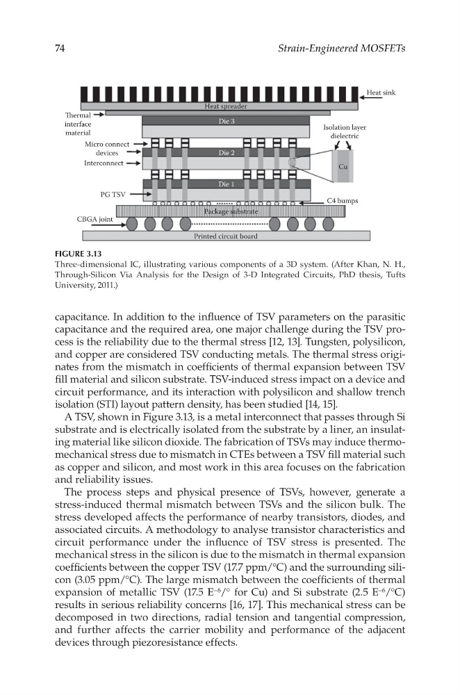
A TSV, shown in Figure 3.13, is a metal interconnect that passes through Si
substrate and is electrically isolated from the substrate by a liner, an insulating material like silicon dioxide. The fabrication of TSVs may induce thermomechanical stress due to mismatch in CTEs between a TSV fill material such
as copper and silicon, and most work in this area focuses on the fabrication
and reliability issues.
The process steps and physical presence of TSVs, however, generate a
stress-induced thermal mismatch between TSVs and the silicon bulk. The
stress developed affects the performance of nearby transistors, diodes, and
associated circuits. A methodology to analyse transistor characteristics and
circuit performance under the influence of TSV stress is presented. The
mechanical stress in the silicon is due to the mismatch in thermal expansion
coefficients between the copper TSV (17.7 ppm/°C) and the surrounding silicon (3.05 ppm/°C). The large mismatch between the coefficients of thermal
expansion of metallic TSV (17.5 E –6 /° for Cu) and Si substrate (2.5 E –6 /°C)
results in serious reliability concerns [16, 17]. This mechanical stress can be
decomposed in two directions, radial tension and tangential compression,
and further affects the carrier mobility and performance of the adjacent
devices through piezoresistance effects.
FIGURE 3.13
Three-dimensional IC, illustrating various components of a 3D system. (After Khan, N. H.,
Through-Silicon Via Analysis for the Design of 3-D Integrated Circuits, PhD thesis, Tufts
University, 2011.)
Strain-Engineered MOSFETs
capacitance. In addition to the influence of TSV parameters on the parasitic
capacitance and the required area, one major challenge during the TSV process is the reliability due to the thermal stress [12, 13]. Tungsten, polysilicon,
and copper are considered TSV conducting metals. The thermal stress originates from the mismatch in coefficients of thermal expansion between TSV
fill material and silicon substrate. TSV-induced stress impact on a device and
circuit performance, and its interaction with polysilicon and shallow trench
isolation (STI) layout pattern density, has been studied [14, 15].
A TSV, shown in Figure 3.13, is a metal interconnect that passes through Si
substrate and is electrically isolated from the substrate by a liner, an insulating material like silicon dioxide. The fabrication of TSVs may induce thermomechanical stress due to mismatch in CTEs between a TSV fill material such
as copper and silicon, and most work in this area focuses on the fabrication
and reliability issues.
The process steps and physical presence of TSVs, however, generate a
stress-induced thermal mismatch between TSVs and the silicon bulk. The
stress developed affects the performance of nearby transistors, diodes, and
associated circuits. A methodology to analyse transistor characteristics and
circuit performance under the influence of TSV stress is presented. The
mechanical stress in the silicon is due to the mismatch in thermal expansion
coefficients between the copper TSV (17.7 ppm/°C) and the surrounding silicon (3.05 ppm/°C). The large mismatch between the coefficients of thermal
expansion of metallic TSV (17.5 E –6 /° for Cu) and Si substrate (2.5 E –6 /°C)
results in serious reliability concerns [16, 17]. This mechanical stress can be
decomposed in two directions, radial tension and tangential compression,
and further affects the carrier mobility and performance of the adjacent
devices through piezoresistance effects.
FIGURE 3.13
Three-dimensional IC, illustrating various components of a 3D system. (After Khan, N. H.,
Through-Silicon Via Analysis for the Design of 3-D Integrated Circuits, PhD thesis, Tufts
University, 2011.)