

69
Process-Induced Stress Engineering in CMOS Technology
SMT technique. Further improvement by combining the SMT with the CESL
technique is also possible.
3.8 Global vs. Local Strain
The global strain technique was one of the first strained Si techniques to be
considered in the CMOS industry, because of its wafer-level applicability. It
consists of a thin silicon layer epitaxially grown onto a Si 1–x Ge x strain-relaxed
buffer (SRB). During its epitaxial growth, the Si layer adopts the lattice constant of the substrate material (Si 1–x Ge x ). Since the Si 1–x Ge x has a bigger lattice
constant than the Si, the formed Si layer is under biaxial tensile strain. The
amount of tensile strain in the grown Si layer depends on the Ge composition
of the relaxed Si 1–x Ge x substrate. It is interesting to note that the hole mobility
Implant
Tensile liner
Tensile liner
RTA
NMOS
P MOS
NMOS
P MOS
Strained NMOS
P MOS
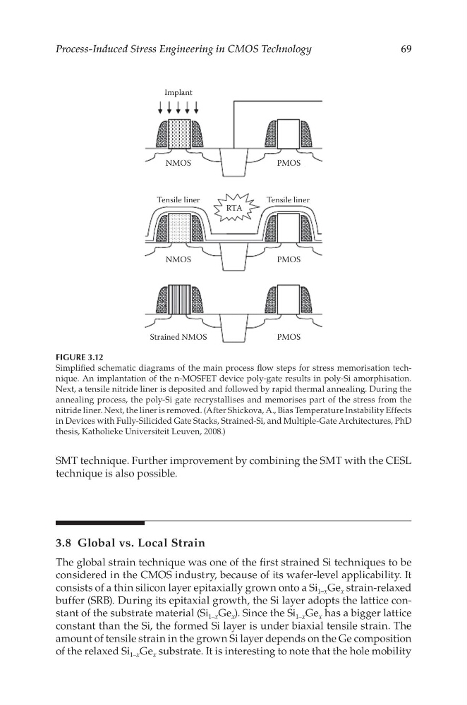
FIGURE 3.12
Simplified schematic diagrams of the main process flow steps for stress memorisation technique. An implantation of the n-MOSFET device poly-gate results in poly-Si amorphisation.
Next, a tensile nitride liner is deposited and followed by rapid thermal annealing. During the
annealing process, the poly-Si gate recrystallises and memorises part of the stress from the
nitride liner. Next, the liner is removed. (After Shickova, A., Bias Temperature Instability Effects
in Devices with Fully-Silicided Gate Stacks, Strained-Si, and Multiple-Gate Architectures, PhD
thesis, Katholieke Universiteit Leuven, 2008.)
Process-Induced Stress Engineering in CMOS Technology
SMT technique. Further improvement by combining the SMT with the CESL
technique is also possible.
3.8 Global vs. Local Strain
The global strain technique was one of the first strained Si techniques to be
considered in the CMOS industry, because of its wafer-level applicability. It
consists of a thin silicon layer epitaxially grown onto a Si 1–x Ge x strain-relaxed
buffer (SRB). During its epitaxial growth, the Si layer adopts the lattice constant of the substrate material (Si 1–x Ge x ). Since the Si 1–x Ge x has a bigger lattice
constant than the Si, the formed Si layer is under biaxial tensile strain. The
amount of tensile strain in the grown Si layer depends on the Ge composition
of the relaxed Si 1–x Ge x substrate. It is interesting to note that the hole mobility
Implant
Tensile liner
Tensile liner
RTA
NMOS
P MOS
NMOS
P MOS
Strained NMOS
P MOS
FIGURE 3.12
Simplified schematic diagrams of the main process flow steps for stress memorisation technique. An implantation of the n-MOSFET device poly-gate results in poly-Si amorphisation.
Next, a tensile nitride liner is deposited and followed by rapid thermal annealing. During the
annealing process, the poly-Si gate recrystallises and memorises part of the stress from the
nitride liner. Next, the liner is removed. (After Shickova, A., Bias Temperature Instability Effects
in Devices with Fully-Silicided Gate Stacks, Strained-Si, and Multiple-Gate Architectures, PhD
thesis, Katholieke Universiteit Leuven, 2008.)