

64
Strain-Engineered MOSFETs
STIW impact, but also builds upon this modelling to improve circuit performance at no area cost.
3.5 Contact Etch Stop Layer (CESL)
The contact etch stop layer technology is a local strain introduction technique
alternative to the Si 1–x Ge x S/D and SiC S/D epitaxial growth techniques. The
CESL technology exploits the intrinsic strain of the nitride contact etch liners
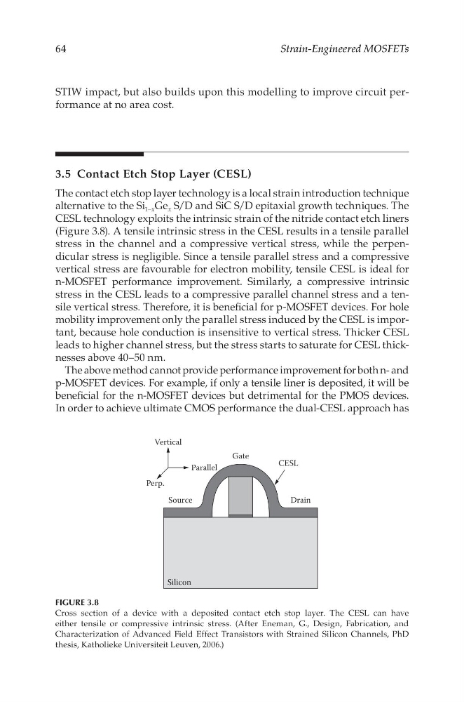
(Figure 3.8). A tensile intrinsic stress in the CESL results in a tensile parallel
stress in the channel and a compressive vertical stress, while the perpendicular stress is negligible. Since a tensile parallel stress and a compressive
vertical stress are favourable for electron mobility, tensile CESL is ideal for
n-MOSFET performance improvement. Similarly, a compressive intrinsic
stress in the CESL leads to a compressive parallel channel stress and a tensile vertical stress. Therefore, it is beneficial for p-MOSFET devices. For hole
mobility improvement only the parallel stress induced by the CESL is important, because hole conduction is insensitive to vertical stress. Thicker CESL
leads to higher channel stress, but the stress starts to saturate for CESL thicknesses above 40–50 nm.
The above method cannot provide performance improvement for both n- and
p-MOSFET devices. For example, if only a tensile liner is deposited, it will be
beneficial for the n-MOSFET devices but detrimental for the PMOS devices.
In order to achieve ultimate CMOS performance the dual-CESL approach has
Drain
CESL
Source
Silicon
Gate
Vertical
Parallel
Perp.
FIGURE 3.8
Cross section of a device with a deposited contact etch stop layer. The CESL can have
either tensile or compressive intrinsic stress. (After Eneman, G., Design, Fabrication, and
Characterization of Advanced Field Effect Transistors with Strained Silicon Channels, PhD
thesis, Katholieke Universiteit Leuven, 2006.)
Strain-Engineered MOSFETs
STIW impact, but also builds upon this modelling to improve circuit performance at no area cost.
3.5 Contact Etch Stop Layer (CESL)
The contact etch stop layer technology is a local strain introduction technique
alternative to the Si 1–x Ge x S/D and SiC S/D epitaxial growth techniques. The
CESL technology exploits the intrinsic strain of the nitride contact etch liners
(Figure 3.8). A tensile intrinsic stress in the CESL results in a tensile parallel
stress in the channel and a compressive vertical stress, while the perpendicular stress is negligible. Since a tensile parallel stress and a compressive
vertical stress are favourable for electron mobility, tensile CESL is ideal for
n-MOSFET performance improvement. Similarly, a compressive intrinsic
stress in the CESL leads to a compressive parallel channel stress and a tensile vertical stress. Therefore, it is beneficial for p-MOSFET devices. For hole
mobility improvement only the parallel stress induced by the CESL is important, because hole conduction is insensitive to vertical stress. Thicker CESL
leads to higher channel stress, but the stress starts to saturate for CESL thicknesses above 40–50 nm.
The above method cannot provide performance improvement for both n- and
p-MOSFET devices. For example, if only a tensile liner is deposited, it will be
beneficial for the n-MOSFET devices but detrimental for the PMOS devices.
In order to achieve ultimate CMOS performance the dual-CESL approach has
Drain
CESL
Source
Silicon
Gate
Vertical
Parallel
Perp.
FIGURE 3.8
Cross section of a device with a deposited contact etch stop layer. The CESL can have
either tensile or compressive intrinsic stress. (After Eneman, G., Design, Fabrication, and
Characterization of Advanced Field Effect Transistors with Strained Silicon Channels, PhD
thesis, Katholieke Universiteit Leuven, 2006.)