

61
Process-Induced Stress Engineering in CMOS Technology
Stress XX
–0.1
0.2
Y (um)
0.1
0
SiGe
Silicon substrate
SiGe
–0.1
0
X (um)
0.1
1.3E+08
–1.0E+09
–2.2E+09
–3.3E+09
–4.5E+09
–5.6E+09
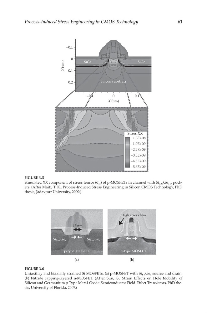
FIGURE 3.5
Simulated XX component of stress tensor (σ xx ) of p-MOSFETs in channel with Si 0.83 Ge 0.17 pockets. (After Maiti, T. K., Process-Induced Stress Engineering in Silicon CMOS Technology, PhD
thesis, Jadavpur University, 2009.)
p-type MOSFET
Si 1–x Ge x
Si 1–x Ge x
45 nm
High stress film
(a)
(b)
n-type MOSFET
FIGURE 3.6
Uniaxillay and biaxially strained Si MOSFETs. (a) p-MOSFET with Si 1–x Ge x source and drain.
(b) Nitride capping-layered n-MOSFET. (After Sun, G., Strain Effects on Hole Mobility of
Silicon and Germanium p-Type Metal-Oxide-Semiconductor Field-Effect-Transistors, PhD thesis, University of Florida, 2007.)
Process-Induced Stress Engineering in CMOS Technology
Stress XX
–0.1
0.2
Y (um)
0.1
0
SiGe
Silicon substrate
SiGe
–0.1
0
X (um)
0.1
1.3E+08
–1.0E+09
–2.2E+09
–3.3E+09
–4.5E+09
–5.6E+09
FIGURE 3.5
Simulated XX component of stress tensor (σ xx ) of p-MOSFETs in channel with Si 0.83 Ge 0.17 pockets. (After Maiti, T. K., Process-Induced Stress Engineering in Silicon CMOS Technology, PhD
thesis, Jadavpur University, 2009.)
p-type MOSFET
Si 1–x Ge x
Si 1–x Ge x
45 nm
High stress film
(a)
(b)
n-type MOSFET
FIGURE 3.6
Uniaxillay and biaxially strained Si MOSFETs. (a) p-MOSFET with Si 1–x Ge x source and drain.
(b) Nitride capping-layered n-MOSFET. (After Sun, G., Strain Effects on Hole Mobility of
Silicon and Germanium p-Type Metal-Oxide-Semiconductor Field-Effect-Transistors, PhD thesis, University of Florida, 2007.)