

56
Strain-Engineered MOSFETs
strain techniques, whereas local techniques induce strain in selected
regions of the wafer. Some of the most prominent strain technologies that
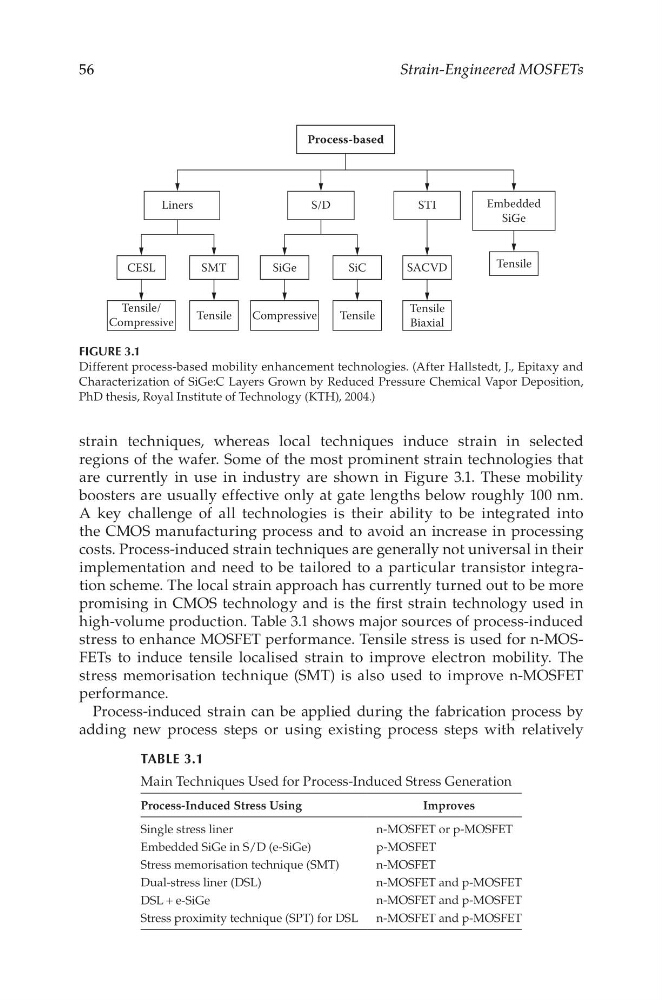
are currently in use in industry are shown in Figure 3.1. These mobility
boosters are usually effective only at gate lengths below roughly 100 nm.
A key challenge of all technologies is their ability to be integrated into
the CMOS manufacturing process and to avoid an increase in processing
costs. Process-induced strain techniques are generally not universal in their
implementation and need to be tailored to a particular transistor integration scheme. The local strain approach has currently turned out to be more
promising in CMOS technology and is the first strain technology used in
high-volume production. Table 3.1 shows major sources of process-induced
stress to enhance MOSFET performance. Tensile stress is used for n-MOSFETs to induce tensile localised strain to improve electron mobility. The
stress memorisation technique (SMT) is also used to improve n-MOSFET
performance.
Process-induced strain can be applied during the fabrication process by
adding new process steps or using existing process steps with relatively
Process-based
Embedded
SiGe
Tensile
Liners
Tensile/
Compressive
CESL
SMT
Tensile
SiGe
SiC
S/D
Tensile
Compressive
SACVD
STI
Tensile
Biaxial
FIGURE 3.1
Different process-based mobility enhancement technologies. (After Hallstedt, J., Epitaxy and
Characterization of SiGe:C Layers Grown by Reduced Pressure Chemical Vapor Deposition,
PhD thesis, Royal Institute of Technology (KTH), 2004.)
TABLE 3.1
Main Techniques Used for Process-Induced Stress Generation
Process-Induced Stress Using
Improves
Single stress liner
n-MOSFET or p-MOSFET
Embedded SiGe in S/D (e-SiGe)
p-MOSFET
Stress memorisation technique (SMT)
n-MOSFET
Dual-stress liner (DSL)
n-MOSFET and p-MOSFET
DSL + e-SiGe
n-MOSFET and p-MOSFET
Stress proximity technique (SPT) for DSL n-MOSFET and p-MOSFET
Strain-Engineered MOSFETs
strain techniques, whereas local techniques induce strain in selected
regions of the wafer. Some of the most prominent strain technologies that
are currently in use in industry are shown in Figure 3.1. These mobility
boosters are usually effective only at gate lengths below roughly 100 nm.
A key challenge of all technologies is their ability to be integrated into
the CMOS manufacturing process and to avoid an increase in processing
costs. Process-induced strain techniques are generally not universal in their
implementation and need to be tailored to a particular transistor integration scheme. The local strain approach has currently turned out to be more
promising in CMOS technology and is the first strain technology used in
high-volume production. Table 3.1 shows major sources of process-induced
stress to enhance MOSFET performance. Tensile stress is used for n-MOSFETs to induce tensile localised strain to improve electron mobility. The
stress memorisation technique (SMT) is also used to improve n-MOSFET
performance.
Process-induced strain can be applied during the fabrication process by
adding new process steps or using existing process steps with relatively
Process-based
Embedded
SiGe
Tensile
Liners
Tensile/
Compressive
CESL
SMT
Tensile
SiGe
SiC
S/D
Tensile
Compressive
SACVD
STI
Tensile
Biaxial
FIGURE 3.1
Different process-based mobility enhancement technologies. (After Hallstedt, J., Epitaxy and
Characterization of SiGe:C Layers Grown by Reduced Pressure Chemical Vapor Deposition,
PhD thesis, Royal Institute of Technology (KTH), 2004.)
TABLE 3.1
Main Techniques Used for Process-Induced Stress Generation
Process-Induced Stress Using
Improves
Single stress liner
n-MOSFET or p-MOSFET
Embedded SiGe in S/D (e-SiGe)
p-MOSFET
Stress memorisation technique (SMT)
n-MOSFET
Dual-stress liner (DSL)
n-MOSFET and p-MOSFET
DSL + e-SiGe
n-MOSFET and p-MOSFET
Stress proximity technique (SPT) for DSL n-MOSFET and p-MOSFET