

50
Strain-Engineered MOSFETs
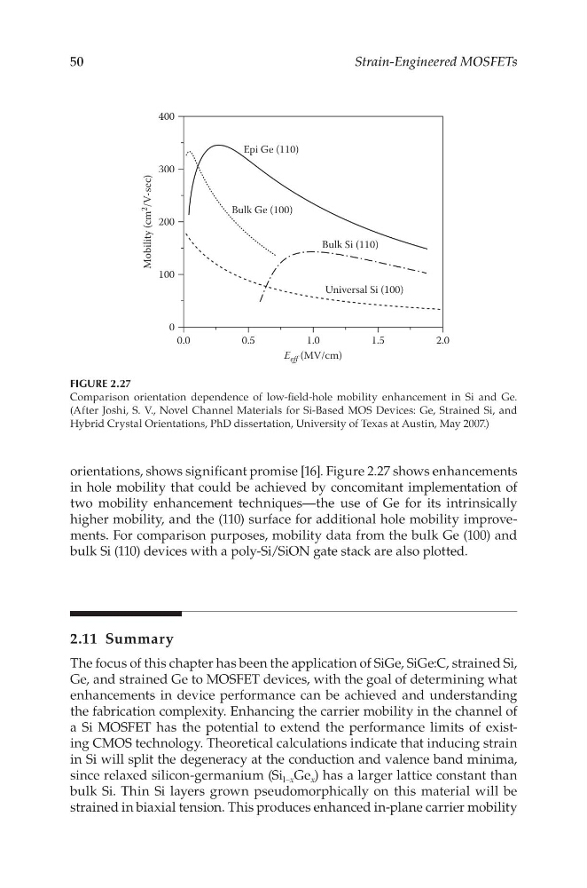
orientations, shows significant promise [16]. Figure 2.27 shows enhancements
in hole mobility that could be achieved by concomitant implementation of
two mobility enhancement techniques—the use of Ge for its intrinsically
higher mobility, and the (110) surface for additional hole mobility improvements. For comparison purposes, mobility data from the bulk Ge (100) and
bulk Si (110) devices with a poly-Si/SiON gate stack are also plotted.
2.11 Summary
The focus of this chapter has been the application of SiGe, SiGe:C, strained Si,
Ge, and strained Ge to MOSFET devices, with the goal of determining what
enhancements in device performance can be achieved and understanding
the fabrication complexity. Enhancing the carrier mobility in the channel of
a Si MOSFET has the potential to extend the performance limits of existing CMOS technology. Theoretical calculations indicate that inducing strain
in Si will split the degeneracy at the conduction and valence band minima,
since relaxed silicon-germanium (Si l–x Ge x ) has a larger lattice constant than
bulk Si. Thin Si layers grown pseudomorphically on this material will be
strained in biaxial tension. This produces enhanced in-plane carrier mobility
400
300
200
Mobility (cm
2
/V-sec)
100
0
0.0
0.5
1.0
Universal Si (100)
Bulk Si (110)
Bulk Ge (100)
Epi Ge (110)
E eff (MV/cm)
1.5
2.0
FIGURE 2.27
Comparison orientation dependence of low-field-hole mobility enhancement in Si and Ge.
(After Joshi, S. V., Novel Channel Materials for Si-Based MOS Devices: Ge, Strained Si, and
Hybrid Crystal Orientations, PhD dissertation, University of Texas at Austin, May 2007.)
Strain-Engineered MOSFETs
orientations, shows significant promise [16]. Figure 2.27 shows enhancements
in hole mobility that could be achieved by concomitant implementation of
two mobility enhancement techniques—the use of Ge for its intrinsically
higher mobility, and the (110) surface for additional hole mobility improvements. For comparison purposes, mobility data from the bulk Ge (100) and
bulk Si (110) devices with a poly-Si/SiON gate stack are also plotted.
2.11 Summary
The focus of this chapter has been the application of SiGe, SiGe:C, strained Si,
Ge, and strained Ge to MOSFET devices, with the goal of determining what
enhancements in device performance can be achieved and understanding
the fabrication complexity. Enhancing the carrier mobility in the channel of
a Si MOSFET has the potential to extend the performance limits of existing CMOS technology. Theoretical calculations indicate that inducing strain
in Si will split the degeneracy at the conduction and valence band minima,
since relaxed silicon-germanium (Si l–x Ge x ) has a larger lattice constant than
bulk Si. Thin Si layers grown pseudomorphically on this material will be
strained in biaxial tension. This produces enhanced in-plane carrier mobility
400
300
200
Mobility (cm
2
/V-sec)
100
0
0.0
0.5
1.0
Universal Si (100)
Bulk Si (110)
Bulk Ge (100)
Epi Ge (110)
E eff (MV/cm)
1.5
2.0
FIGURE 2.27
Comparison orientation dependence of low-field-hole mobility enhancement in Si and Ge.
(After Joshi, S. V., Novel Channel Materials for Si-Based MOS Devices: Ge, Strained Si, and
Hybrid Crystal Orientations, PhD dissertation, University of Texas at Austin, May 2007.)