

48
Strain-Engineered MOSFETs
mobility, the proper channel direction and substrate orientation have to be
chosen to obtain the maximum mobility enhancement. In the hybrid orientation technology, which is based on wafer bonding techniques and selective epitaxy, the larger carrier mobility of holes for (110)-oriented substrate is
exploited to enhance the performance of p-MOSFETs. HOT seems promising
because processes are directly compatible with existing CMOS technology
and strain engineering. Let us consider the architecture of the transistor in
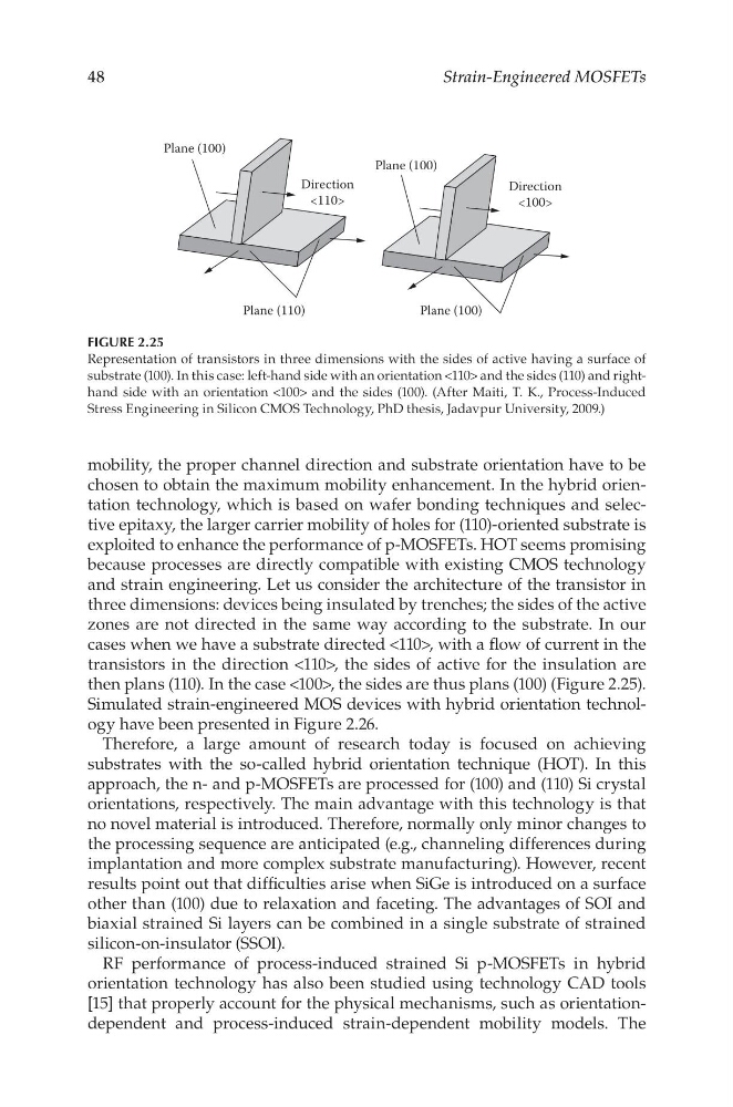
three dimensions: devices being insulated by trenches; the sides of the active
zones are not directed in the same way according to the substrate. In our
cases when we have a substrate directed <110>, with a flow of current in the
transistors in the direction <110>, the sides of active for the insulation are
then plans (110). In the case <100>, the sides are thus plans (100) (Figure 2.25).
Simulated strain-engineered MOS devices with hybrid orientation technology have been presented in Figure 2.26.
Therefore, a large amount of research today is focused on achieving
substrates with the so-called hybrid orientation technique (HOT). In this
approach, the n- and p-MOSFETs are processed for (100) and (110) Si crystal
orientations, respectively. The main advantage with this technology is that
no novel material is introduced. Therefore, normally only minor changes to
the processing sequence are anticipated (e.g., channeling differences during
implantation and more complex substrate manufacturing). However, recent
results point out that difficulties arise when SiGe is introduced on a surface
other than (100) due to relaxation and faceting. The advantages of SOI and
biaxial strained Si layers can be combined in a single substrate of strained
silicon-on-insulator (SSOI).
RF performance of process-induced strained Si p-MOSFETs in hybrid
orientation technology has also been studied using technology CAD tools
[15] that properly account for the physical mechanisms, such as orientationdependent and process-induced strain-dependent mobility models. The
Plane (100)
Plane (100)
Plane (100)
Plane (110)
Direction
<110>
Direction
<100>
FIGURE 2.25
Representation of transistors in three dimensions with the sides of active having a surface of
substrate (100). In this case: left-hand side with an orientation <110> and the sides (110) and righthand side with an orientation <100> and the sides (100). (After Maiti, T. K., Process-Induced
Stress Engineering in Silicon CMOS Technology, PhD thesis, Jadavpur University, 2009.)
Strain-Engineered MOSFETs
mobility, the proper channel direction and substrate orientation have to be
chosen to obtain the maximum mobility enhancement. In the hybrid orientation technology, which is based on wafer bonding techniques and selective epitaxy, the larger carrier mobility of holes for (110)-oriented substrate is
exploited to enhance the performance of p-MOSFETs. HOT seems promising
because processes are directly compatible with existing CMOS technology
and strain engineering. Let us consider the architecture of the transistor in
three dimensions: devices being insulated by trenches; the sides of the active
zones are not directed in the same way according to the substrate. In our
cases when we have a substrate directed <110>, with a flow of current in the
transistors in the direction <110>, the sides of active for the insulation are
then plans (110). In the case <100>, the sides are thus plans (100) (Figure 2.25).
Simulated strain-engineered MOS devices with hybrid orientation technology have been presented in Figure 2.26.
Therefore, a large amount of research today is focused on achieving
substrates with the so-called hybrid orientation technique (HOT). In this
approach, the n- and p-MOSFETs are processed for (100) and (110) Si crystal
orientations, respectively. The main advantage with this technology is that
no novel material is introduced. Therefore, normally only minor changes to
the processing sequence are anticipated (e.g., channeling differences during
implantation and more complex substrate manufacturing). However, recent
results point out that difficulties arise when SiGe is introduced on a surface
other than (100) due to relaxation and faceting. The advantages of SOI and
biaxial strained Si layers can be combined in a single substrate of strained
silicon-on-insulator (SSOI).
RF performance of process-induced strained Si p-MOSFETs in hybrid
orientation technology has also been studied using technology CAD tools
[15] that properly account for the physical mechanisms, such as orientationdependent and process-induced strain-dependent mobility models. The
Plane (100)
Plane (100)
Plane (100)
Plane (110)
Direction
<110>
Direction
<100>
FIGURE 2.25
Representation of transistors in three dimensions with the sides of active having a surface of
substrate (100). In this case: left-hand side with an orientation <110> and the sides (110) and righthand side with an orientation <100> and the sides (100). (After Maiti, T. K., Process-Induced
Stress Engineering in Silicon CMOS Technology, PhD thesis, Jadavpur University, 2009.)