

47
Substrate-Induced Strain Engineering in CMOS Technology
1
400
500
600
pFET I on (µA/µm)
700
10
100
29%
1000
pFET I
off (nA/µm)
(110)/<110> compressive
(110)/<100> compressive
(110)/<110> neutral
(110)/<100> neutral
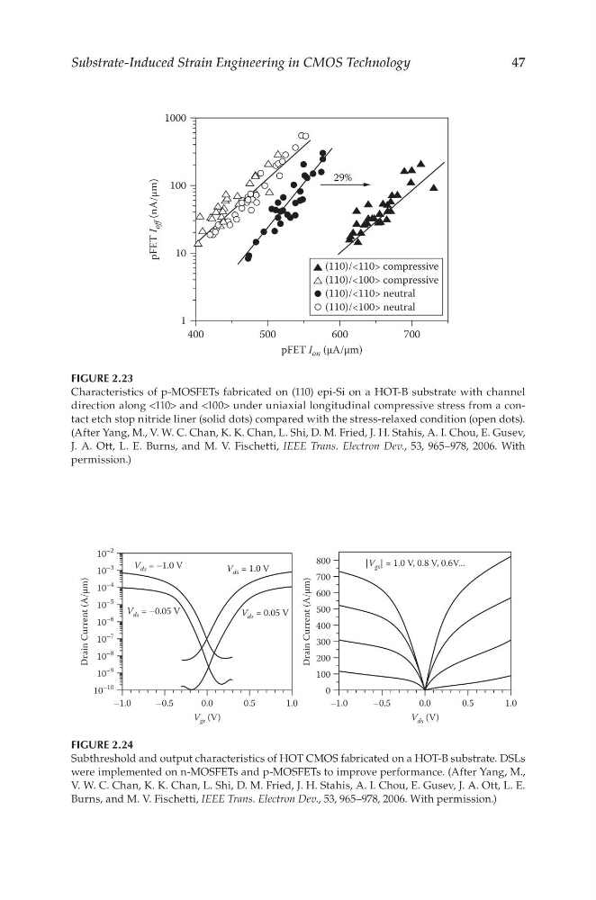
FIGURE 2.23
Characteristics of p-MOSFETs fabricated on (110) epi-Si on a HOT-B substrate with channel
direction along <110> and <100> under uniaxial longitudinal compressive stress from a contact etch stop nitride liner (solid dots) compared with the stress-relaxed condition (open dots).
(After Yang, M., V. W. C. Chan, K. K. Chan, L. Shi, D. M. Fried, J. H. Stahis, A. I. Chou, E. Gusev,
J. A. Ott, L. E. Burns, and M. V. Fischetti, IEEE Trans. Electron Dev., 53, 965–978, 2006. With
permission.)
10
–10
–1.0
–0.5
0.0
V gs (V)
V ds = –0.05 V
V ds = 0.05 V
|V gs | = 1.0 V, 0.8 V, 0.6V...
V ds = –1.0 V
V ds = 1.0 V
0.5
1.0
–1.0
–0.5
0.0
V ds (V)
0.5
1.0
Drain Current (A/µm)
10
–9
10
–8
10
–7
10
–6
10
–5
10
–4
10
–3
10
–2
0
Drain Current (A/µm)
200
100
300
400
500
600
700
800
FIGURE 2.24
Subthreshold and output characteristics of HOT CMOS fabricated on a HOT-B substrate. DSLs
were implemented on n-MOSFETs and p-MOSFETs to improve performance. (After Yang, M.,
V. W. C. Chan, K. K. Chan, L. Shi, D. M. Fried, J. H. Stahis, A. I. Chou, E. Gusev, J. A. Ott, L. E.
Burns, and M. V. Fischetti, IEEE Trans. Electron Dev., 53, 965–978, 2006. With permission.)
Substrate-Induced Strain Engineering in CMOS Technology
1
400
500
600
pFET I on (µA/µm)
700
10
100
29%
1000
pFET I
off (nA/µm)
(110)/<110> compressive
(110)/<100> compressive
(110)/<110> neutral
(110)/<100> neutral
FIGURE 2.23
Characteristics of p-MOSFETs fabricated on (110) epi-Si on a HOT-B substrate with channel
direction along <110> and <100> under uniaxial longitudinal compressive stress from a contact etch stop nitride liner (solid dots) compared with the stress-relaxed condition (open dots).
(After Yang, M., V. W. C. Chan, K. K. Chan, L. Shi, D. M. Fried, J. H. Stahis, A. I. Chou, E. Gusev,
J. A. Ott, L. E. Burns, and M. V. Fischetti, IEEE Trans. Electron Dev., 53, 965–978, 2006. With
permission.)
10
–10
–1.0
–0.5
0.0
V gs (V)
V ds = –0.05 V
V ds = 0.05 V
|V gs | = 1.0 V, 0.8 V, 0.6V...
V ds = –1.0 V
V ds = 1.0 V
0.5
1.0
–1.0
–0.5
0.0
V ds (V)
0.5
1.0
Drain Current (A/µm)
10
–9
10
–8
10
–7
10
–6
10
–5
10
–4
10
–3
10
–2
0
Drain Current (A/µm)
200
100
300
400
500
600
700
800
FIGURE 2.24
Subthreshold and output characteristics of HOT CMOS fabricated on a HOT-B substrate. DSLs
were implemented on n-MOSFETs and p-MOSFETs to improve performance. (After Yang, M.,
V. W. C. Chan, K. K. Chan, L. Shi, D. M. Fried, J. H. Stahis, A. I. Chou, E. Gusev, J. A. Ott, L. E.
Burns, and M. V. Fischetti, IEEE Trans. Electron Dev., 53, 965–978, 2006. With permission.)