

45
Substrate-Induced Strain Engineering in CMOS Technology
The combination of dual-stress liners (DSLs) with HOT provides excellent
CMOS performance, with a record p-MOSFET drive current of 730 μA/μm at
90 nA/μm I off and –1.0 V supply voltage. The subthreshold and output characteristics of p- and n-MOSFET are given in Figure 2.24. The subthreshold
slope is 96 and 108 mV/dec, and drain-induced barrier lowering (DIBL) is 102
and 147 mV for p- and n-MOSFET, respectively.
2.10.1 Device Simulation
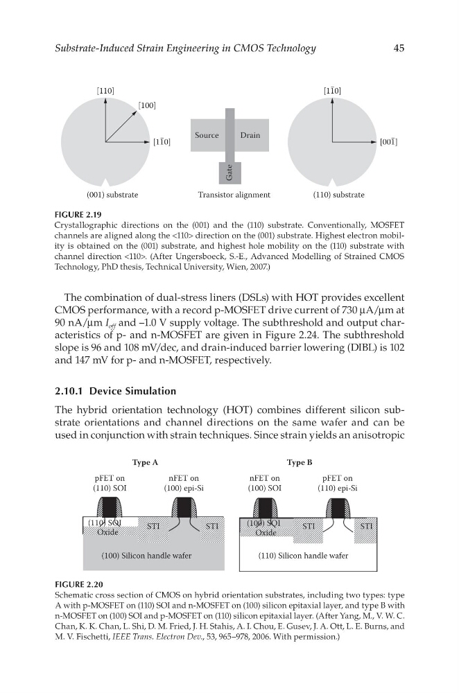
The hybrid orientation technology (HOT) combines different silicon substrate orientations and channel directions on the same wafer and can be
used in conjunction with strain techniques. Since strain yields an anisotropic
(001) substrate
(110) substrate
Transistor alignment
[110]
[110]
[100]
Source
Drain
Gate
[001]
[110]
FIGURE 2.19
Crystallographic directions on the (001) and the (110) substrate. Conventionally, MOSFET
channels are aligned along the <110> direction on the (001) substrate. Highest electron mobility is obtained on the (001) substrate, and highest hole mobility on the (110) substrate with
channel direction <110>. (After Ungersboeck, S.-E., Advanced Modelling of Strained CMOS
Technology, PhD thesis, Technical University, Wien, 2007.)
(110) Silicon handle wafer
(100) Silicon handle wafer
STI
(100) SOI
Oxide
Oxide
(110) SOI
STI
STI
S TI
pFET on
(110) epi-Si
nFET on
(100) epi-Si
pFET on
(110) SOI
Type A
T ype B
nFET on
(100) SOI
FIGURE 2.20
Schematic cross section of CMOS on hybrid orientation substrates, including two types: type
A with p-MOSFET on (110) SOI and n-MOSFET on (100) silicon epitaxial layer, and type B with
n-MOSFET on (100) SOI and p-MOSFET on (110) silicon epitaxial layer. (After Yang, M., V. W. C.
Chan, K. K. Chan, L. Shi, D. M. Fried, J. H. Stahis, A. I. Chou, E. Gusev, J. A. Ott, L. E. Burns, and
M. V. Fischetti, IEEE Trans. Electron Dev., 53, 965–978, 2006. With permission.)
Substrate-Induced Strain Engineering in CMOS Technology
The combination of dual-stress liners (DSLs) with HOT provides excellent
CMOS performance, with a record p-MOSFET drive current of 730 μA/μm at
90 nA/μm I off and –1.0 V supply voltage. The subthreshold and output characteristics of p- and n-MOSFET are given in Figure 2.24. The subthreshold
slope is 96 and 108 mV/dec, and drain-induced barrier lowering (DIBL) is 102
and 147 mV for p- and n-MOSFET, respectively.
2.10.1 Device Simulation
The hybrid orientation technology (HOT) combines different silicon substrate orientations and channel directions on the same wafer and can be
used in conjunction with strain techniques. Since strain yields an anisotropic
(001) substrate
(110) substrate
Transistor alignment
[110]
[110]
[100]
Source
Drain
Gate
[001]
[110]
FIGURE 2.19
Crystallographic directions on the (001) and the (110) substrate. Conventionally, MOSFET
channels are aligned along the <110> direction on the (001) substrate. Highest electron mobility is obtained on the (001) substrate, and highest hole mobility on the (110) substrate with
channel direction <110>. (After Ungersboeck, S.-E., Advanced Modelling of Strained CMOS
Technology, PhD thesis, Technical University, Wien, 2007.)
(110) Silicon handle wafer
(100) Silicon handle wafer
STI
(100) SOI
Oxide
Oxide
(110) SOI
STI
STI
S TI
pFET on
(110) epi-Si
nFET on
(100) epi-Si
pFET on
(110) SOI
Type A
T ype B
nFET on
(100) SOI
FIGURE 2.20
Schematic cross section of CMOS on hybrid orientation substrates, including two types: type
A with p-MOSFET on (110) SOI and n-MOSFET on (100) silicon epitaxial layer, and type B with
n-MOSFET on (100) SOI and p-MOSFET on (110) silicon epitaxial layer. (After Yang, M., V. W. C.
Chan, K. K. Chan, L. Shi, D. M. Fried, J. H. Stahis, A. I. Chou, E. Gusev, J. A. Ott, L. E. Burns, and
M. V. Fischetti, IEEE Trans. Electron Dev., 53, 965–978, 2006. With permission.)