

42
Strain-Engineered MOSFETs
Observation of hole mobility enhancement in strained Si p-MOSFETs was
first demonstrated by Nayak et al. [11]. The initial devices were fabricated
on a 1 μm thick uniform-composition partially relaxed SiGe buffer, which is
known to have a very high defect density, which resulted in a limited performance (subthreshold slope 111 mV/decade). An improved device structure
and process to fabricate high-performance strained Si p-MOSFETs with a
step-graded completely relaxed thick (3 μm) SiGe buffer layer (defect density < 10 5 cm –2 ), a low thermal budget (maximum temperature 700°C), and
a high-quality (100 Å) gate oxide has been reported. As discussed earlier,
strained Si is more difficult to grow than strained Si 1–x Ge x , since bulk Si 1–x Ge x
substrate is currently not available and, until recently, growth of relaxed
Si 1–x Ge x without forming a large concentration of defects due to dislocations
was difficult. Moreover, the thermal budget of a conventional CMOS process, which is largely dominated by the gate oxide growth and annealing
process steps, needs to be minimised for the fabrication of strained Si/SiGe
devices. Optimisation of the thermal budget is necessary because significant
Ge outdiffusion and corresponding strain relaxation at process temperatures
beyond 800°C are observed.
Problems arising from the dislocations include (1) reduction of carrier
mobility due to scattering, which consequently lowers the operating speed
of devices, (2) dopant diffusions along dislocation lines that cause current
1000
800
600
400
200
0
0
0.1
300 K
Si control
Ge fraction
0
0.10
0.20
0.29
L G = 10 µm V DS = 10 mV
0.2
0.3
E eff (MV/cm)
µ
eff cm
2
/Vs)
0.4
0.5
0.6
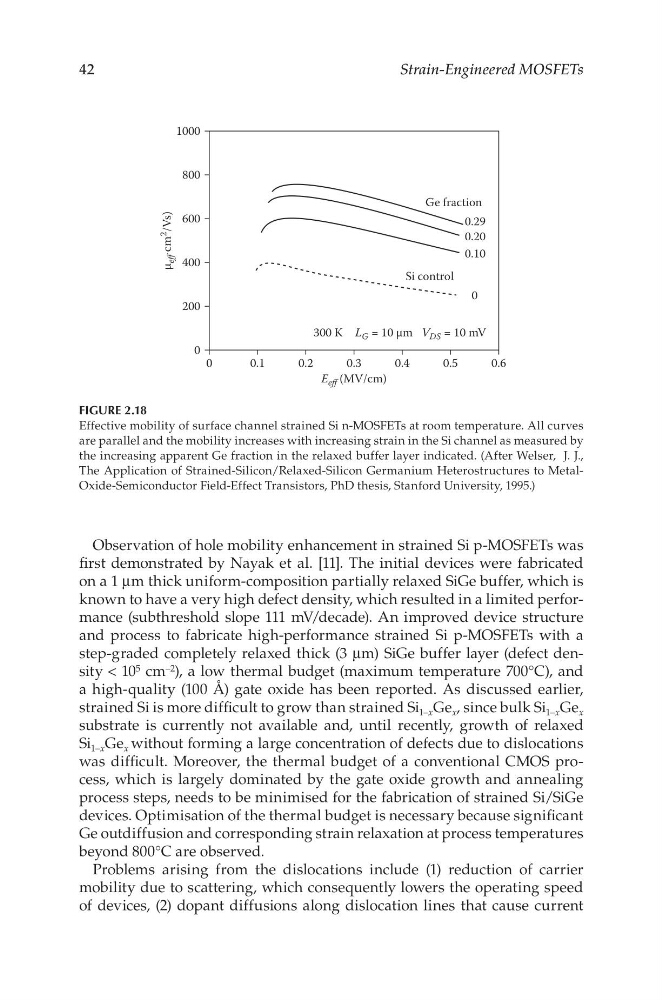
FIGURE 2.18
Effective mobility of surface channel strained Si n-MOSFETs at room temperature. All curves
are parallel and the mobility increases with increasing strain in the Si channel as measured by
the increasing apparent Ge fraction in the relaxed buffer layer indicated. (After Welser, J. J.,
The Application of Strained-Silicon/Relaxed-Silicon Germanium Heterostructures to MetalOxide-Semiconductor Field-Effect Transistors, PhD thesis, Stanford University, 1995.)
Strain-Engineered MOSFETs
Observation of hole mobility enhancement in strained Si p-MOSFETs was
first demonstrated by Nayak et al. [11]. The initial devices were fabricated
on a 1 μm thick uniform-composition partially relaxed SiGe buffer, which is
known to have a very high defect density, which resulted in a limited performance (subthreshold slope 111 mV/decade). An improved device structure
and process to fabricate high-performance strained Si p-MOSFETs with a
step-graded completely relaxed thick (3 μm) SiGe buffer layer (defect density < 10 5 cm –2 ), a low thermal budget (maximum temperature 700°C), and
a high-quality (100 Å) gate oxide has been reported. As discussed earlier,
strained Si is more difficult to grow than strained Si 1–x Ge x , since bulk Si 1–x Ge x
substrate is currently not available and, until recently, growth of relaxed
Si 1–x Ge x without forming a large concentration of defects due to dislocations
was difficult. Moreover, the thermal budget of a conventional CMOS process, which is largely dominated by the gate oxide growth and annealing
process steps, needs to be minimised for the fabrication of strained Si/SiGe
devices. Optimisation of the thermal budget is necessary because significant
Ge outdiffusion and corresponding strain relaxation at process temperatures
beyond 800°C are observed.
Problems arising from the dislocations include (1) reduction of carrier
mobility due to scattering, which consequently lowers the operating speed
of devices, (2) dopant diffusions along dislocation lines that cause current
1000
800
600
400
200
0
0
0.1
300 K
Si control
Ge fraction
0
0.10
0.20
0.29
L G = 10 µm V DS = 10 mV
0.2
0.3
E eff (MV/cm)
µ
eff cm
2
/Vs)
0.4
0.5
0.6
FIGURE 2.18
Effective mobility of surface channel strained Si n-MOSFETs at room temperature. All curves
are parallel and the mobility increases with increasing strain in the Si channel as measured by
the increasing apparent Ge fraction in the relaxed buffer layer indicated. (After Welser, J. J.,
The Application of Strained-Silicon/Relaxed-Silicon Germanium Heterostructures to MetalOxide-Semiconductor Field-Effect Transistors, PhD thesis, Stanford University, 1995.)