

41
Substrate-Induced Strain Engineering in CMOS Technology
both larger conduction and valence band offsets and does not suffer from
alloy scattering (hence mobility degradation). The significant improvement
in both electron and hole mobility shows the possibility of both n- and p-type
FET devices for strained Si/SiGe-based heterostructure CMOS (HCMOS)
technology.
First-generation strained Si MOSFETs were all based on SiGe virtual
substrates. The strained Si n-MOSFET grown on SiGe virtual substrate to
improve electron mobility was first demonstrated by J. J. Welser in 1992. In
the experiment, strained Si channel was grown on relaxed Si 0.71 Ge 0.29 layers,
which were on top of the graded buffer layer. The mobility of the strained
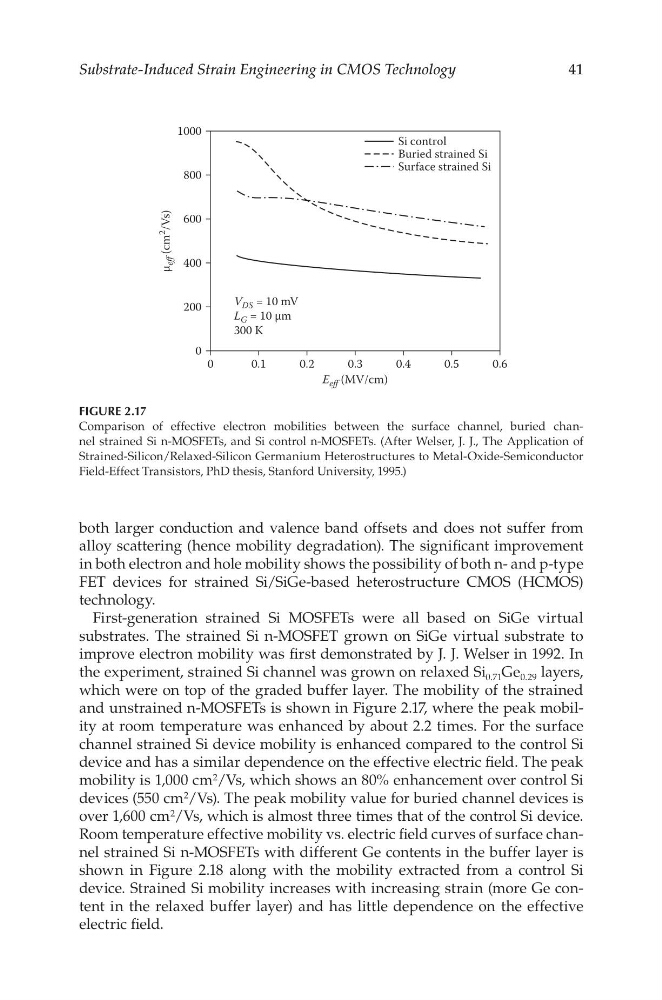
and unstrained n-MOSFETs is shown in Figure 2.17, where the peak mobility at room temperature was enhanced by about 2.2 times. For the surface
channel strained Si device mobility is enhanced compared to the control Si
device and has a similar dependence on the effective electric field. The peak
mobility is 1,000 cm 2 /Vs, which shows an 80% enhancement over control Si
devices (550 cm 2 /Vs). The peak mobility value for buried channel devices is
over 1,600 cm 2 /Vs, which is almost three times that of the control Si device.
Room temperature effective mobility vs. electric field curves of surface channel strained Si n-MOSFETs with different Ge contents in the buffer layer is
shown in Figure 2.18 along with the mobility extracted from a control Si
device. Strained Si mobility increases with increasing strain (more Ge content in the relaxed buffer layer) and has little dependence on the effective
electric field.
1000
800
Si control
Buried strained Si
Surface strained Si
600
400
µ
eff (cm
2
/Vs)
200
0
0
0.1
V DS = 10 mV
L G = 10 µm
300 K
0.2
0.3
E eff (MV/cm)
0.4
0.5
0.6
FIGURE 2.17
Comparison of effective electron mobilities between the surface channel, buried channel strained Si n-MOSFETs, and Si control n-MOSFETs. (After Welser, J. J., The Application of
Strained-Silicon/Relaxed-Silicon Germanium Heterostructures to Metal-Oxide-Semiconductor
Field-Effect Transistors, PhD thesis, Stanford University, 1995.)
Substrate-Induced Strain Engineering in CMOS Technology
both larger conduction and valence band offsets and does not suffer from
alloy scattering (hence mobility degradation). The significant improvement
in both electron and hole mobility shows the possibility of both n- and p-type
FET devices for strained Si/SiGe-based heterostructure CMOS (HCMOS)
technology.
First-generation strained Si MOSFETs were all based on SiGe virtual
substrates. The strained Si n-MOSFET grown on SiGe virtual substrate to
improve electron mobility was first demonstrated by J. J. Welser in 1992. In
the experiment, strained Si channel was grown on relaxed Si 0.71 Ge 0.29 layers,
which were on top of the graded buffer layer. The mobility of the strained
and unstrained n-MOSFETs is shown in Figure 2.17, where the peak mobility at room temperature was enhanced by about 2.2 times. For the surface
channel strained Si device mobility is enhanced compared to the control Si
device and has a similar dependence on the effective electric field. The peak
mobility is 1,000 cm 2 /Vs, which shows an 80% enhancement over control Si
devices (550 cm 2 /Vs). The peak mobility value for buried channel devices is
over 1,600 cm 2 /Vs, which is almost three times that of the control Si device.
Room temperature effective mobility vs. electric field curves of surface channel strained Si n-MOSFETs with different Ge contents in the buffer layer is
shown in Figure 2.18 along with the mobility extracted from a control Si
device. Strained Si mobility increases with increasing strain (more Ge content in the relaxed buffer layer) and has little dependence on the effective
electric field.
1000
800
Si control
Buried strained Si
Surface strained Si
600
400
µ
eff (cm
2
/Vs)
200
0
0
0.1
V DS = 10 mV
L G = 10 µm
300 K
0.2
0.3
E eff (MV/cm)
0.4
0.5
0.6
FIGURE 2.17
Comparison of effective electron mobilities between the surface channel, buried channel strained Si n-MOSFETs, and Si control n-MOSFETs. (After Welser, J. J., The Application of
Strained-Silicon/Relaxed-Silicon Germanium Heterostructures to Metal-Oxide-Semiconductor
Field-Effect Transistors, PhD thesis, Stanford University, 1995.)