

38
Strain-Engineered MOSFETs
In their work on the DQW SiGe, Yousif [9] extended the possibilities of
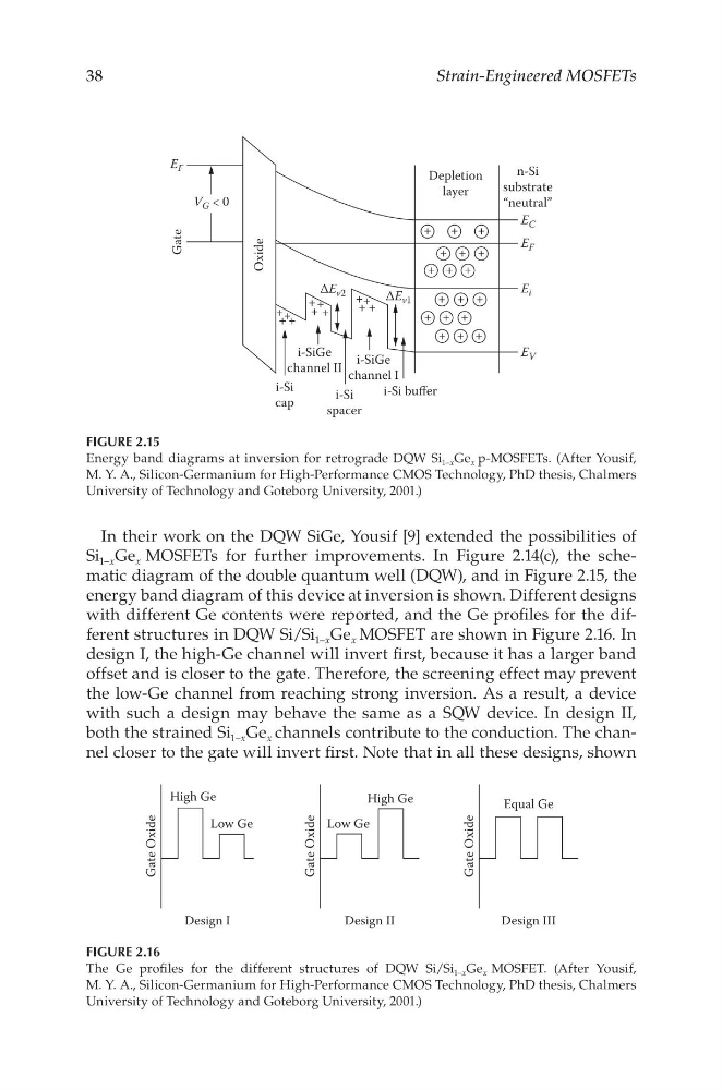
Si 1–x Ge x MOSFETs for further improvements. In Figure 2.14(c), the schematic diagram of the double quantum well (DQW), and in Figure 2.15, the
energy band diagram of this device at inversion is shown. Different designs
with different Ge contents were reported, and the Ge profiles for the different structures in DQW Si/Si 1–x Ge x MOSFET are shown in Figure 2.16. In
design I, the high-Ge channel will invert first, because it has a larger band
offset and is closer to the gate. Therefore, the screening effect may prevent
the low-Ge channel from reaching strong inversion. As a result, a device
with such a design may behave the same as a SQW device. In design II,
both the strained Si 1–x Ge x channels contribute to the conduction. The channel closer to the gate will invert first. Note that in all these designs, shown
Depletion
layer
n-Si
substrate
“neutral”
Oxide
Gate
+
+ + +
+ + +
+ + +
+ + +
+ + +
+ +
i-Si
cap
i-SiGe
channel II
∆E v2
∆E v1
E V
E i
E F
E C
+ + +
+
++
+ +
+ +
+
+
i-SiGe
channel I
i-Si
spacer
i-Si buffer
V G < 0
E F
FIGURE 2.15
Energy band diagrams at inversion for retrograde DQW Si 1–x Ge x p-MOSFETs. (After Yousif,
M. Y. A., Silicon-Germanium for High-Performance CMOS Technology, PhD thesis, Chalmers
University of Technology and Goteborg University, 2001.)
Design I
High Ge
Low Ge
Gate Oxide
Design II
High Ge
Low Ge
Gate Oxide
Design III
Equal Ge
Gate Oxide
FIGURE 2.16
The Ge profiles for the different structures of DQW Si/Si 1–x Ge x MOSFET. (After Yousif,
M. Y. A., Silicon-Germanium for High-Performance CMOS Technology, PhD thesis, Chalmers
University of Technology and Goteborg University, 2001.)
Strain-Engineered MOSFETs
In their work on the DQW SiGe, Yousif [9] extended the possibilities of
Si 1–x Ge x MOSFETs for further improvements. In Figure 2.14(c), the schematic diagram of the double quantum well (DQW), and in Figure 2.15, the
energy band diagram of this device at inversion is shown. Different designs
with different Ge contents were reported, and the Ge profiles for the different structures in DQW Si/Si 1–x Ge x MOSFET are shown in Figure 2.16. In
design I, the high-Ge channel will invert first, because it has a larger band
offset and is closer to the gate. Therefore, the screening effect may prevent
the low-Ge channel from reaching strong inversion. As a result, a device
with such a design may behave the same as a SQW device. In design II,
both the strained Si 1–x Ge x channels contribute to the conduction. The channel closer to the gate will invert first. Note that in all these designs, shown
Depletion
layer
n-Si
substrate
“neutral”
Oxide
Gate
+
+ + +
+ + +
+ + +
+ + +
+ + +
+ +
i-Si
cap
i-SiGe
channel II
∆E v2
∆E v1
E V
E i
E F
E C
+ + +
+
++
+ +
+ +
+
+
i-SiGe
channel I
i-Si
spacer
i-Si buffer
V G < 0
E F
FIGURE 2.15
Energy band diagrams at inversion for retrograde DQW Si 1–x Ge x p-MOSFETs. (After Yousif,
M. Y. A., Silicon-Germanium for High-Performance CMOS Technology, PhD thesis, Chalmers
University of Technology and Goteborg University, 2001.)
Design I
High Ge
Low Ge
Gate Oxide
Design II
High Ge
Low Ge
Gate Oxide
Design III
Equal Ge
Gate Oxide
FIGURE 2.16
The Ge profiles for the different structures of DQW Si/Si 1–x Ge x MOSFET. (After Yousif,
M. Y. A., Silicon-Germanium for High-Performance CMOS Technology, PhD thesis, Chalmers
University of Technology and Goteborg University, 2001.)