

34
Strain-Engineered MOSFETs
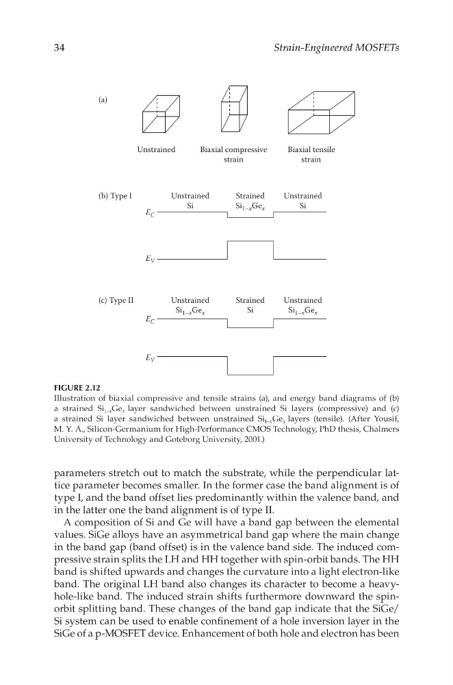
parameters stretch out to match the substrate, while the perpendicular lattice parameter becomes smaller. In the former case the band alignment is of
type I, and the band offset lies predominantly within the valence band, and
in the latter one the band alignment is of type II.
A composition of Si and Ge will have a band gap between the elemental
values. SiGe alloys have an asymmetrical band gap where the main change
in the band gap (band offset) is in the valence band side. The induced compressive strain splits the LH and HH together with spin-orbit bands. The HH
band is shifted upwards and changes the curvature into a light electron-like
band. The original LH band also changes its character to become a heavyhole-like band. The induced strain shifts furthermore downward the spinorbit splitting band. These changes of the band gap indicate that the SiGe/
Si system can be used to enable confinement of a hole inversion layer in the
SiGe of a p-MOSFET device. Enhancement of both hole and electron has been
Unstrained
(a)
(b) Type I
(c) Type II
Unstrained
Si
E C
E V
E C
E V
Unstrained
Si
Strained
Si 1–x Ge x
Unstrained
Si 1–x Ge x
Unstrained
Si 1–x Ge x
Strained
Si
Biaxial compressive
strain
Biaxial tensile
strain
FIGURE 2.12
Illustration of biaxial compressive and tensile strains (a), and energy band diagrams of (b)
a strained Si 1–x Ge x layer sandwiched between unstrained Si layers (compressive) and (c)
a strained Si layer sandwiched between unstrained Si 1–x Ge x layers (tensile). (After Yousif,
M. Y. A., Silicon-Germanium for High-Performance CMOS Technology, PhD thesis, Chalmers
University of Technology and Goteborg University, 2001.)
Strain-Engineered MOSFETs
parameters stretch out to match the substrate, while the perpendicular lattice parameter becomes smaller. In the former case the band alignment is of
type I, and the band offset lies predominantly within the valence band, and
in the latter one the band alignment is of type II.
A composition of Si and Ge will have a band gap between the elemental
values. SiGe alloys have an asymmetrical band gap where the main change
in the band gap (band offset) is in the valence band side. The induced compressive strain splits the LH and HH together with spin-orbit bands. The HH
band is shifted upwards and changes the curvature into a light electron-like
band. The original LH band also changes its character to become a heavyhole-like band. The induced strain shifts furthermore downward the spinorbit splitting band. These changes of the band gap indicate that the SiGe/
Si system can be used to enable confinement of a hole inversion layer in the
SiGe of a p-MOSFET device. Enhancement of both hole and electron has been
Unstrained
(a)
(b) Type I
(c) Type II
Unstrained
Si
E C
E V
E C
E V
Unstrained
Si
Strained
Si 1–x Ge x
Unstrained
Si 1–x Ge x
Unstrained
Si 1–x Ge x
Strained
Si
Biaxial compressive
strain
Biaxial tensile
strain
FIGURE 2.12
Illustration of biaxial compressive and tensile strains (a), and energy band diagrams of (b)
a strained Si 1–x Ge x layer sandwiched between unstrained Si layers (compressive) and (c)
a strained Si layer sandwiched between unstrained Si 1–x Ge x layers (tensile). (After Yousif,
M. Y. A., Silicon-Germanium for High-Performance CMOS Technology, PhD thesis, Chalmers
University of Technology and Goteborg University, 2001.)