

32
Strain-Engineered MOSFETs
currents are 20 μA/μm for p-MOSFET and 10 μA/μm for n-MOSFET at |V g − V T |
= 1.2 V. n-Channel MOSFETs show a lower drive current than p-MOSFETs, and
this may be attributed to intervalley scattering and defect scattering in the Si
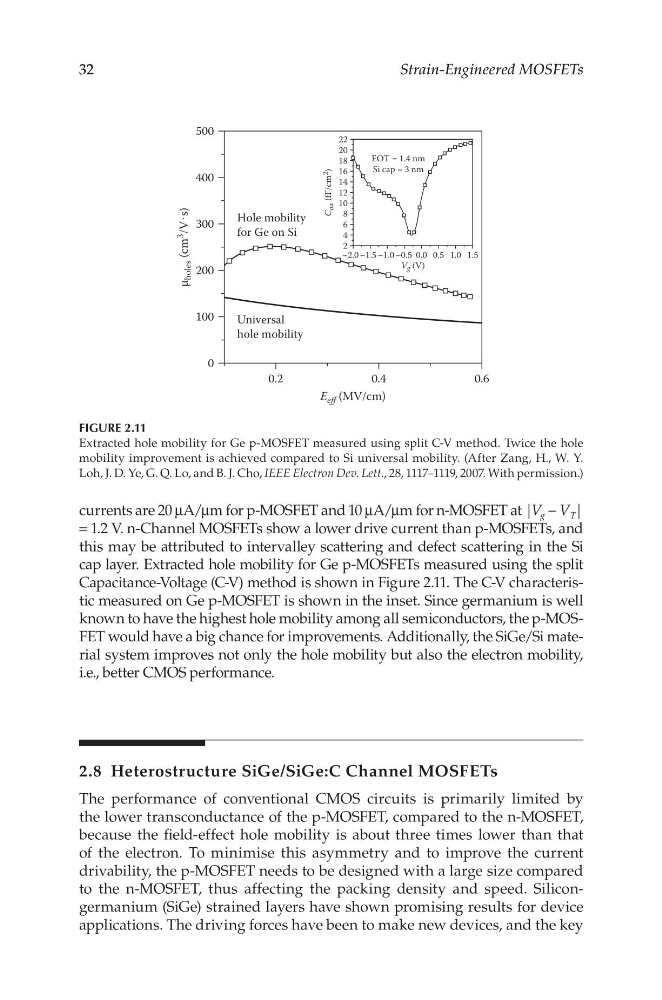
cap layer. Extracted hole mobility for Ge p-MOSFETs measured using the split
Capacitance-Voltage (C-V) method is shown in Figure 2.11. The C-V characteristic measured on Ge p-MOSFET is shown in the inset. Since germanium is well
known to have the highest hole mobility among all semiconductors, the p-MOSFET would have a big chance for improvements. Additionally, the SiGe/Si material system improves not only the hole mobility but also the electron mobility,
i.e., better CMOS performance.
2.8 Heterostructure SiGe/SiGe:C Channel MOSFETs
The performance of conventional CMOS circuits is primarily limited by
the lower transconductance of the p-MOSFET, compared to the n-MOSFET,
because the field-effect hole mobility is about three times lower than that
of the electron. To minimise this asymmetry and to improve the current
drivability, the p-MOSFET needs to be designed with a large size compared
to the n-MOSFET, thus affecting the packing density and speed. Silicongermanium (SiGe) strained layers have shown promising results for device
applications. The driving forces have been to make new devices, and the key
0
0.2
0.4
E eff (MV/cm)
0.6
100
Universal
hole mobility
Hole mobility
for Ge on Si
C
ox (fF/cm 2
)
200
µ
holes (cm
3
/V s)
300
400
22
20
18
16
14
EOT = 1.4 nm
Si cap = 3 nm
12
10
8
6
4
2
–2.0 –1.5 –1.0 –0.5
V g (V)
0.0 0.5 1.0 1.5
500
FIGURE 2.11
Extracted hole mobility for Ge p-MOSFET measured using split C-V method. Twice the hole
mobility improvement is achieved compared to Si universal mobility. (After Zang, H., W. Y.
Loh, J. D. Ye, G. Q. Lo, and B. J. Cho, IEEE Electron Dev. Lett., 28, 1117–1119, 2007. With permission.)
Strain-Engineered MOSFETs
currents are 20 μA/μm for p-MOSFET and 10 μA/μm for n-MOSFET at |V g − V T |
= 1.2 V. n-Channel MOSFETs show a lower drive current than p-MOSFETs, and
this may be attributed to intervalley scattering and defect scattering in the Si
cap layer. Extracted hole mobility for Ge p-MOSFETs measured using the split
Capacitance-Voltage (C-V) method is shown in Figure 2.11. The C-V characteristic measured on Ge p-MOSFET is shown in the inset. Since germanium is well
known to have the highest hole mobility among all semiconductors, the p-MOSFET would have a big chance for improvements. Additionally, the SiGe/Si material system improves not only the hole mobility but also the electron mobility,
i.e., better CMOS performance.
2.8 Heterostructure SiGe/SiGe:C Channel MOSFETs
The performance of conventional CMOS circuits is primarily limited by
the lower transconductance of the p-MOSFET, compared to the n-MOSFET,
because the field-effect hole mobility is about three times lower than that
of the electron. To minimise this asymmetry and to improve the current
drivability, the p-MOSFET needs to be designed with a large size compared
to the n-MOSFET, thus affecting the packing density and speed. Silicongermanium (SiGe) strained layers have shown promising results for device
applications. The driving forces have been to make new devices, and the key
0
0.2
0.4
E eff (MV/cm)
0.6
100
Universal
hole mobility
Hole mobility
for Ge on Si
C
ox (fF/cm 2
)
200
µ
holes (cm
3
/V s)
300
400
22
20
18
16
14
EOT = 1.4 nm
Si cap = 3 nm
12
10
8
6
4
2
–2.0 –1.5 –1.0 –0.5
V g (V)
0.0 0.5 1.0 1.5
500
FIGURE 2.11
Extracted hole mobility for Ge p-MOSFET measured using split C-V method. Twice the hole
mobility improvement is achieved compared to Si universal mobility. (After Zang, H., W. Y.
Loh, J. D. Ye, G. Q. Lo, and B. J. Cho, IEEE Electron Dev. Lett., 28, 1117–1119, 2007. With permission.)