

31
Substrate-Induced Strain Engineering in CMOS Technology
the fabricated MOSFETs are far from a defect-rich region. Due to epi-Si passivation on Ge, the leakage current of HfO 2 is 10 −4 to 10 −5 A/cm 2 at |V g | = 1 V.
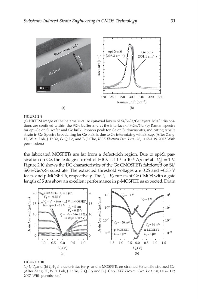
Figure 2.10 shows the DC characteristics of the Ge CMOSFETs fabricated on Si/
SiGe/Ge/s-Si substrate. The extracted threshold voltages are 0.25 and −0.35 V
for n- and p-MOSFETs, respectively. The I d − V d curves of Ge CMOS with a gate
length of 5 μm show an excellent performance in p-MOSFET, as expected. Drain
270
Intensity (a.u.)
epi Ge/Si
(298.3 cm
–1 )
Ge bulk
(301.1 cm
–1 )
280 290 300
Raman Shift (cm
–1 )
(b)
(a)
2 7 9 n m
100 nm
G e la y e r
P a s s iv a t io n o x id e
310 320 330
FIGURE 2.9
(a) HRTEM image of the heterostructure epitaxial layers of Si/SiGe/Ge layers. Misfit dislocations are confined within the SiGe buffer and at the interface of SiGe/Ge. (b) Raman spectra
for epi-Ge on Si wafer and Ge bulk. Phonon peak for Ge on Si downshifts, indicating tensile
strain in Ge. Spectra broadening for Ge on Si is due to Ge intermixing with Si cap. (After Zang,
H., W. Y. Loh, J. D. Ye, G. Q. Lo, and B. J. Cho, IEEE Electron Dev. Lett., 28, 1117–1119, 2007. With
permission.)
–1.0
0
Drain Current (µA/µm)
5
10
15
20
10 –2
Drain Current (µA/µm)
10
–1
10
0
10
1
10
–2
10
–1
10
0
10
1
0
5
10
15
20
p-MOSFET L g = 5 µm
V T = –0.35 V
V g – V T = 0 to –1.2 V n-MOSFET,
in steps of –0.2 V L g = 5 µm
V T = 0.25 V
V g – V T = 0 to 1.2 V
in steps of 0.2 V
V d = –1 V
V d = –50 mV
V d = 50 mV
L g = 5 µm
L g = 5 µm
n-MOSFET
p-MOSFET
V d = 1 V
–0.5 0.0
V D (V)
(a)
0.5
1.0
–1.0
–1.5
–0.5 0.0
V G (V)
(b)
0.5 1.0 1.5
FIGURE 2.10
(a) I d -V d and (b) I d -V g characteristics for p- and n-MOSFETs on strained Si/tensile-strained Ge.
(After Zang, H., W. Y. Loh, J. D. Ye, G. Q. Lo, and B. J. Cho, IEEE Electron Dev. Lett., 28, 1117–1119,
2007. With permission.)
Substrate-Induced Strain Engineering in CMOS Technology
the fabricated MOSFETs are far from a defect-rich region. Due to epi-Si passivation on Ge, the leakage current of HfO 2 is 10 −4 to 10 −5 A/cm 2 at |V g | = 1 V.
Figure 2.10 shows the DC characteristics of the Ge CMOSFETs fabricated on Si/
SiGe/Ge/s-Si substrate. The extracted threshold voltages are 0.25 and −0.35 V
for n- and p-MOSFETs, respectively. The I d − V d curves of Ge CMOS with a gate
length of 5 μm show an excellent performance in p-MOSFET, as expected. Drain
270
Intensity (a.u.)
epi Ge/Si
(298.3 cm
–1 )
Ge bulk
(301.1 cm
–1 )
280 290 300
Raman Shift (cm
–1 )
(b)
(a)
2 7 9 n m
100 nm
G e la y e r
P a s s iv a t io n o x id e
310 320 330
FIGURE 2.9
(a) HRTEM image of the heterostructure epitaxial layers of Si/SiGe/Ge layers. Misfit dislocations are confined within the SiGe buffer and at the interface of SiGe/Ge. (b) Raman spectra
for epi-Ge on Si wafer and Ge bulk. Phonon peak for Ge on Si downshifts, indicating tensile
strain in Ge. Spectra broadening for Ge on Si is due to Ge intermixing with Si cap. (After Zang,
H., W. Y. Loh, J. D. Ye, G. Q. Lo, and B. J. Cho, IEEE Electron Dev. Lett., 28, 1117–1119, 2007. With
permission.)
–1.0
0
Drain Current (µA/µm)
5
10
15
20
10 –2
Drain Current (µA/µm)
10
–1
10
0
10
1
10
–2
10
–1
10
0
10
1
0
5
10
15
20
p-MOSFET L g = 5 µm
V T = –0.35 V
V g – V T = 0 to –1.2 V n-MOSFET,
in steps of –0.2 V L g = 5 µm
V T = 0.25 V
V g – V T = 0 to 1.2 V
in steps of 0.2 V
V d = –1 V
V d = –50 mV
V d = 50 mV
L g = 5 µm
L g = 5 µm
n-MOSFET
p-MOSFET
V d = 1 V
–0.5 0.0
V D (V)
(a)
0.5
1.0
–1.0
–1.5
–0.5 0.0
V G (V)
(b)
0.5 1.0 1.5
FIGURE 2.10
(a) I d -V d and (b) I d -V g characteristics for p- and n-MOSFETs on strained Si/tensile-strained Ge.
(After Zang, H., W. Y. Loh, J. D. Ye, G. Q. Lo, and B. J. Cho, IEEE Electron Dev. Lett., 28, 1117–1119,
2007. With permission.)