

24
Strain-Engineered MOSFETs
use a graded composition of 1–2 μm/10%Ge. The approach depends largely
on materials engineering rather than device design. The strain stretches the
silicon lattice by about 1%. This technology is rather mature and dislocation
densities on the order of 10 5 cm –2 can be obtained. The main drawback of this
grading Ge method is the growth of thick buffer layers, which suffers from
long deposition times and large material consumption. The epitaxial growth
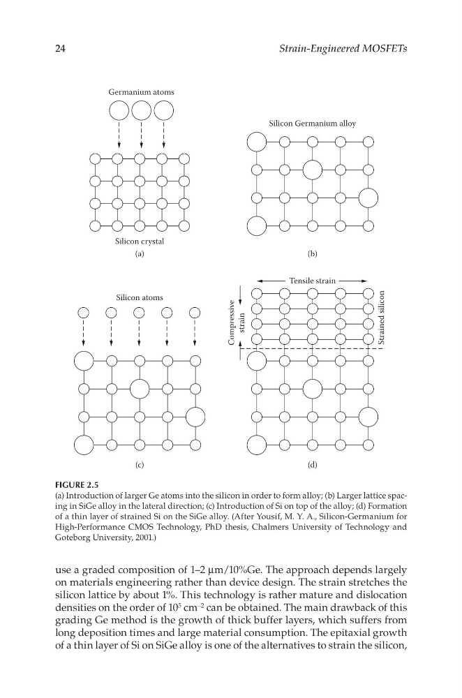
of a thin layer of Si on SiGe alloy is one of the alternatives to strain the silicon,
Germanium atoms
Silicon crystal
(a)
(c)
(d)
(b)
Silicon Germanium alloy
Silicon atoms
Tensile strain
Compressive
strain
Strained silicon
FIGURE 2.5
(a) Introduction of larger Ge atoms into the silicon in order to form alloy; (b) Larger lattice spacing in SiGe alloy in the lateral direction; (c) Introduction of Si on top of the alloy; (d) Formation
of a thin layer of strained Si on the SiGe alloy. (After Yousif, M. Y. A., Silicon-Germanium for
High-Performance CMOS Technology, PhD thesis, Chalmers University of Technology and
Goteborg University, 2001.)
Strain-Engineered MOSFETs
use a graded composition of 1–2 μm/10%Ge. The approach depends largely
on materials engineering rather than device design. The strain stretches the
silicon lattice by about 1%. This technology is rather mature and dislocation
densities on the order of 10 5 cm –2 can be obtained. The main drawback of this
grading Ge method is the growth of thick buffer layers, which suffers from
long deposition times and large material consumption. The epitaxial growth
of a thin layer of Si on SiGe alloy is one of the alternatives to strain the silicon,
Germanium atoms
Silicon crystal
(a)
(c)
(d)
(b)
Silicon Germanium alloy
Silicon atoms
Tensile strain
Compressive
strain
Strained silicon
FIGURE 2.5
(a) Introduction of larger Ge atoms into the silicon in order to form alloy; (b) Larger lattice spacing in SiGe alloy in the lateral direction; (c) Introduction of Si on top of the alloy; (d) Formation
of a thin layer of strained Si on the SiGe alloy. (After Yousif, M. Y. A., Silicon-Germanium for
High-Performance CMOS Technology, PhD thesis, Chalmers University of Technology and
Goteborg University, 2001.)